4-2-5
RF
FILTER CIRCUIT (PA
UNIT)
The
PA UNIT has 6
Chebyshev low-pass
filters. The
signal from the
power
amplifier
(Q5, Q6),
applied to
one of
the low-pass
filters depending on the transmit
frequency
range,
suppresses high
harmonic components.
The
filter switching voltage,
obtained at the
PLL UNIT, is
applied to
the
PA
UNIT via P7.
FREQUENCIES AND
APPROPRIATE
FILTERS
FILTER FREQUENCY RANGE
(MHz)
LI
Below 2
L2
2~4
L3
1
CO
L4
8~15
L5
15~22
L6
22-30
The
filtered signal passes
through the SWR detector
circuit (L51)
and is then
applied
to
the antenna connector.
The
forward signal
from
L51
is detected
at
D7 and
applied
to the
MAIN UNIT as the
“FOR” voltage.
The reflection
signal from L51 is detected
at D8 and applied to the
MAIN
UNIT as the
“REF” voltage.
4-2-6
ALC CIRCUIT
(MAIN UNIT)
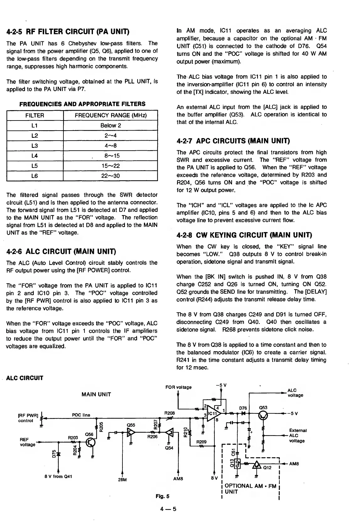
The ALC
(Auto Level
Control) circuit stably controls the
RF output power
using
the
[RF POWER]
control.
The “FOR” voltage from
the PA UNIT is applied to IC11
pin 2 and IC10
pin
3.
The “POC” voltage
controlled
by
the [RF PWR] control
is also applied
to
IC1
1
pin 3 as
the
reference voltage.
When the “FOR” voltage
exceeds the “POC” voltage, ALC
bias voltage from IC11
pin 1 controls the IF
amplifiers
to
reduce the output power
until the “FOR” and “POC”
voltages
are equalized.
In AM mode, IC11
operates
as an
averaging
ALC
amplifier, because a
capacitor on the optional AM
•
FM
UNIT
(C51)
is connected to the cathode
of
D76. Q54
turns ON and
the “POC” voltage
is shifted for 40 W AM
output power
(maximum).
The
ALC bias voltage from
IC11 pin 1 is also applied
to
the
inversion-amplifier (IC1
1
pin
6)
to
control an intensity
of
the [TX] indicator, showing the ALC level.
An external
ALC input from the [ALC] jack is
applied
to
the
buffer amplifier
(Q53).
ALC
operation is identical
to
that of the internal ALC.
4-2-7
APC CIRCUITS
(MAIN UNIT)
The APC circuits
protect the final transistors from high
SWR and
excessive current. The “REF” voltage
from
the
PA UNIT is applied to Q56.
When
the
“REF” voltage
exceeds
the reference voltage,
determined by R203 and
R204, Q56
turns ON and the “POC” voltage is
shifted
for 12 W output power.
The
“ICH” and “ICL” voltages
are applied to the Ic APC
amplifier
(IC10,
pins
5
and
6)
and then to the ALC bias
voltage
line
to prevent excessive current flow.
4-2-8
CW KEYING
CIRCUIT (MAIN UNIT)
When the
CW
key is
closed, the “KEY” signal line
becomes “LOW.”
Q38
outputs
8
V
to
control break-in
operation, sidetone
signal and transmit signal.
When the [BK IN] switch is
pushed
IN, 8
V from
Q38
charge
C252
and
026
is turned ON,
turning ON Q52.
Q52
grounds the SEND line
for transmitting. The [DELAY]
control (R244) adjusts the
transmit release
delay
time.
The 8 V
from
038
charges
C249
and
D91
is turned OFF,
disconnecting
C249
from 040. 040 then oscillates a
sidetone
signal.
R268
prevents sidetone
click noise.
TTie
8
V from 038 is applied to a
time
constant
and then
to
the balanced modulator (IC6) to create a
carrier signal.
R241
in
the time constant adjusts a
transmit
delay
timing
for 12 msec.
ALC
CIRCUIT
4
—
5