4 - 5
4-5 OTHER CIRCUITS
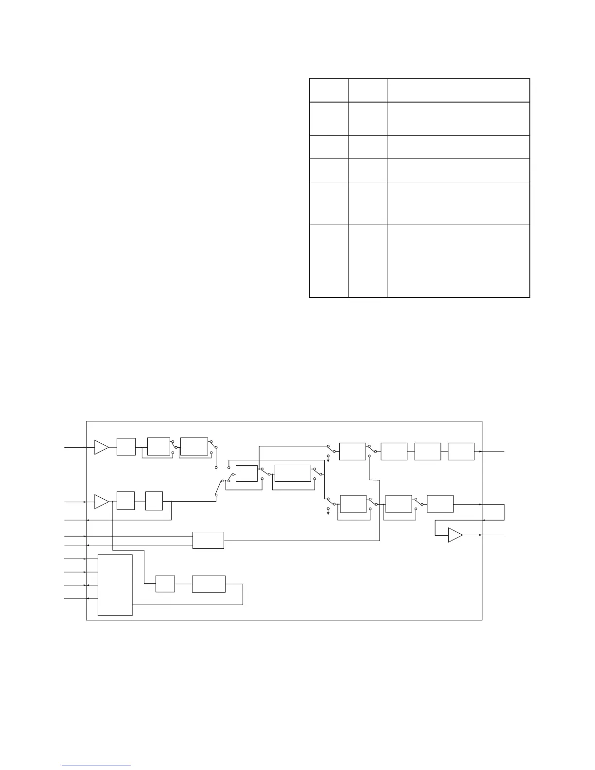
4-5-1 COMPANDER CIRCUIT (MAIN UNIT)
IC-F33GT/GS/F34GT/GS have compander circuit which can
improve S/N ratio and become wide dynamic range. The cir-
cuit is composed in the base band IC (IC14).
(1) IN CASE OF TRANSMITTING
The audio signals from the microphone are applied to the
base band IC (IC14, pin 3) via microphone amplifier (IC23).
The signals are amplified at the amplifier section, and are
then applied to the compressor circuit to compress the audio
signals. The signals pass through (or bypass) scrambler sec-
tion, and are then applied to the limiter section after being
passed through the high-pass filter. The filtered signals pass
through the splatter filter section, and are then applied to the
modulation circuit (D12) via the FM/PM switch (IC13), low-
pass filter (IC6) and D/A converter (IC12).
(2) IN CASE OF RECEIVING
The demodulated AF signals from the IF IC are applied to
the amplifier section in base band IC (IC14, pin 23), and
then pass through the low-pass and high-pass filter sec-
tion to suppress unwanted signals. The filtered signals pass
through (or bypass) scrambler section, and are then applied
to the expander circuit to expand AF signals. The signals are
applied to the base band IC’s amplifier section (IC14, pins
19, 20), and are then applied to the AF amplifier circuit.
Pin
Number
Port
name
Description
10 BAL
Outputs the modulation balance level
control signal. The signal is applied to
the buffer amplifi er (IC24, pin 1).
14 TLVA
Outputs the TX VCO lock voltage
control signal.
15 RLVA
Outputs the RX VCO lock voltage
control signal.
22
T1
Outputs the bandpass filter tuning
control signal . The output signal is
applied to the bandpass fi lters (D19,
D240).
23 T2
• Outputs the bandpass filter tuning
control signal . The output signal is
applied to the bandpass fi lters (D14,
D15).
• Outputs the TX control signal . The
output signal is applied to the APC
amplifi er (IC2, pin 1).
Scrambler/
De-scrambler
TX/RX
HPF
Pre-
emphasis
Limiter Splatter VR2
Expander VR4
RXA2
SMF
De-
emphasis
Com-
pressor
VR1
(HPF)
RX
LPF
VR3
(HPF)
7 MOD
18
19
20 SIGNAL
3TXIN
23RXIN
21SDEC
10
14MDIR
9
MTDT
MTCK
13MSCK
11MDIO
12MRDF
MSK
Modulator
MSK
Demodulator
MSK
BPF
Control
Register
TXA1
RXA1
4-6 PORT ALLOCATIONS
4-6-1 D/A CONVERTOR IC (IC12)
• BASE BAND IC BLOCK DIAGRAM
 Loading...