Application Note 8 2011-07-06
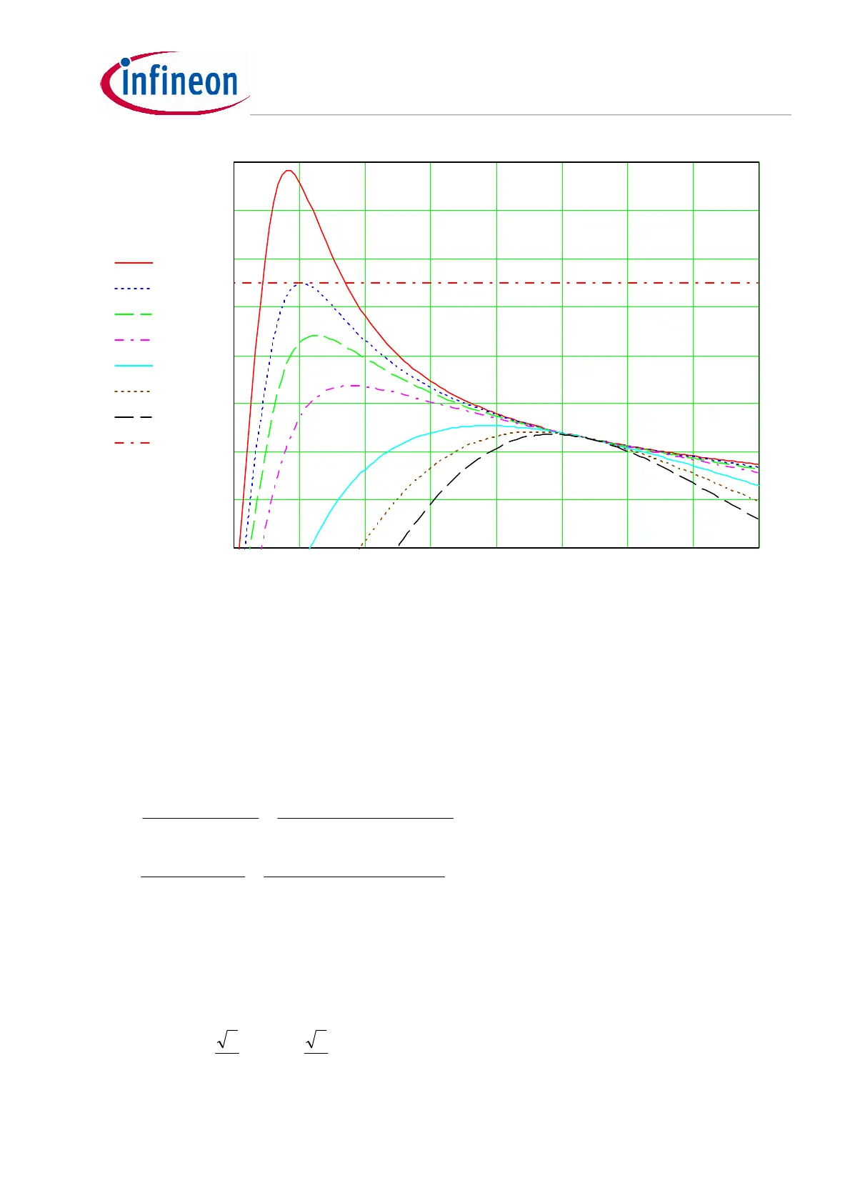
Figure 2 Voltage gain G Vs normalized frequency F
Among the curves, we find that the one with
267.0
Q can achieve the required peak gain
pk
G , which
is 8% higher than
max
M for design margin, i.e.
28.108.1
max
== MG
pk
From the curve, the corresponding
35.0
min
F can be located where 28.1
pk
G is achieved.
Having found the proper
Q , we can calculate the
r
C
,
r
L
and
p
L as follows:
nF
RfQ
C
effr
r
66
106*10*85*268.0*2
1
***2
1
3
===
π
π
[8]
uH
Cf
L
rr
r
53
10*66*)10*85*2(
1
*)*2(
1
9232
===
−
ππ
[9]
uHmLL
rp
690==
2.2.6.1 Resonant choke design
The minimum rms voltage across the resonant network is:
[10]
Then the corresponding rms current flowing through the resonant choke
r
L
can be calculated as:
0.2 0.35 0.5 0.65 0.8 0.95 1.1 1.25 1.4
0.8
0.888
0.975
1.063
1.15
1.238
1.325
1.413
1.5
GF0.22, ()
GF0.267, ()
GF0.3, ()
GF0.35, ()
GF0.5, ()
GF0.65, ()
GF0.8, ()
Line
F
VVV
inrmsin
79.1512.337*
22
min_min__
===
ππ
 Loading...