1/0
INTERFACING
ADDRESS
=[]s
LINE
10RC
.Rii
110
DEVICE
10WC
WR
A15
A14
(A)
ONE
CHIP
SELECT
CS
CS
Rii
--<:
WR
CS
CS
Rii
WR
(8)
MULTIPLE
CHIP
SELECTS
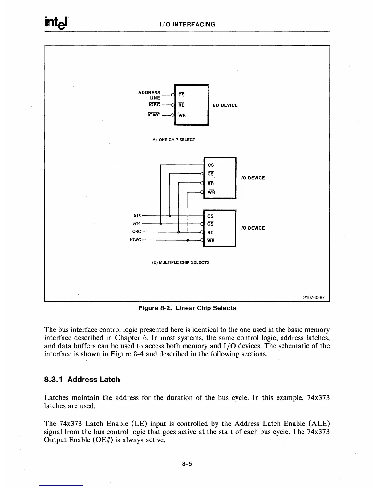
Figure 8-2. Linear Chip
Selects
110
DEVICE
110
DEVICE
210760-97
The
bus
interface control logic presented here
is
identical to the one used
in
the basic memory
interface described
in
Chapter
6.
In most systems, the same control logic, address latches,
and data buffers can be used
to
access both memory and
I/O
devices. The schematic of the
interface
is
shown in Figure 8-4 and described in the following sections.
8.3.1 Address Latch
Latches maintain the address for the duration of the bus cycle. In this example, 74x373
latches are used.
The 74x373 Latch Enable (LE) input
is
controlled
by
the Address Latch Enable (ALE)
signal from the bus control logic that
goes
active at the start of each bus cycle. The 74x373
Output Enable
(OE#)
is
always active.
8-5