1/0
INTERFACING
I
BUS
CONTROL
ADDRESS
I
~
LOGIC
-
---l\,
DECODER
WAIT·STATE
GENERATOR
--V
~
1/0
---vI
DEVICE
#1
~
-
I---+-
rV
ADDRESS
r>
LATCH
READY#
BUS
STATUS
-
I---+-
ADDRESS
...
80386
)
1/0
DEVICE
~
#2
DATA
A
...
TRANSCEIVER
DATA
...
....
"
G30107
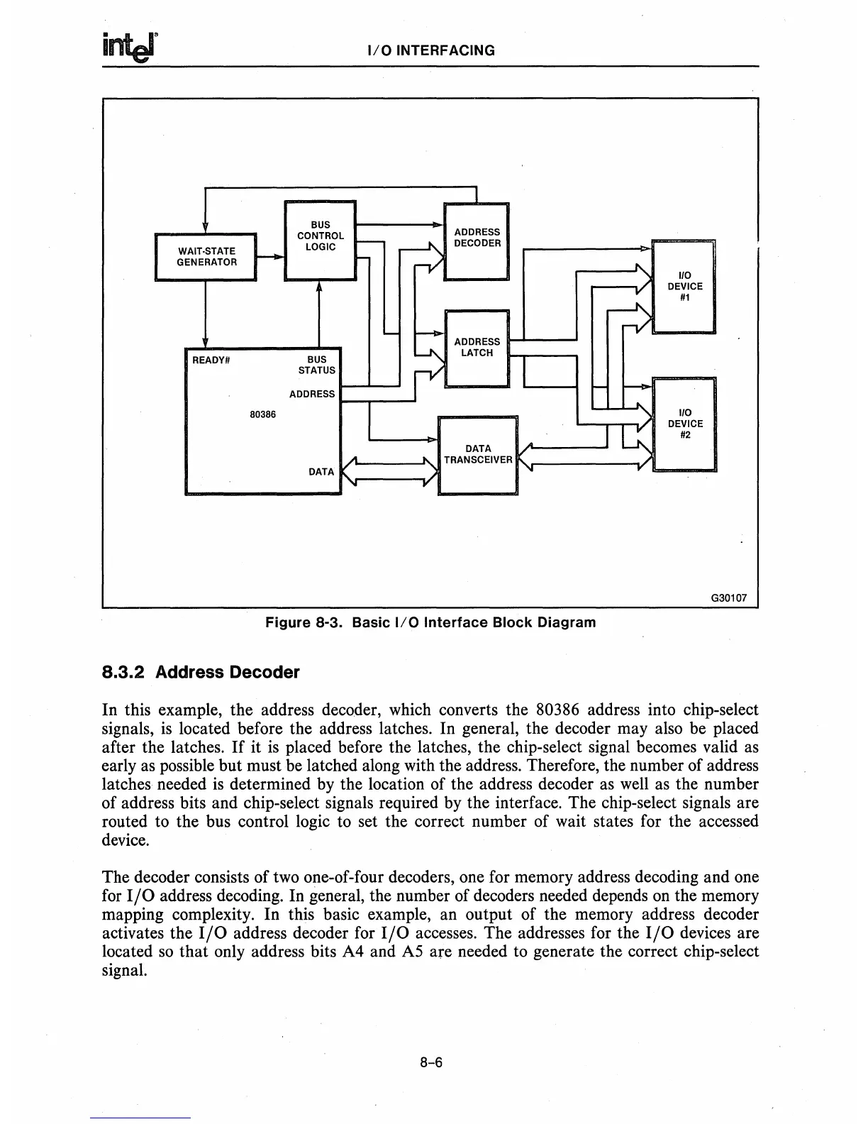
Figure
8-3. Basic
1/0
Interface
Block
Diagram
8.3.2
Address Decoder
In this example, the address decoder, which converts the 80386 address into chip-select
signals,
is
located before the address latches. In general, the decoder may also be placed
after the latches.
If
it
is
placed before the latches, the chip-select signal becomes valid
as
early
as
possible but must be latched along with the address. Therefore, the number of address
latches needed
is
determined
by
the location of the address decoder
as
well
as
the number
of address bits and chip-select signals required
by
the interface. The chip-select signals are
routed to the bus control logic to set the correct number of wait states for the accessed
device.
The decoder consists of two one-of-four decoders, one for memory address decoding and one
for
I/O
address decoding. In general, the number of decoders needed depends
on
the memory
mapping complexity. In this basic example, an output of the memory address decoder
activates the
I/O
address decoder for
I/O
accesses. The addresses for the
I/O
devices are
located
so
that only address bits A4 and
AS
are needed to generate the correct chip-select
signal.
8-6