inter
PHYSICAL DESIGN AND DEBUGGING
Decoupling capacitors placed across the device between
Vee
and ground reduce voltage spikes
by supplying the extra current needed during switching. These capacitors should be placed
close to their devices because the inductance of connection lines negates their effect.
When selecting decoupling capacitors, the user should provide
0.01
microfarads for each
device and
0.1
microfarads for every
20
gates. Radio-frequency capacitors must be used;
they should be distributed evenly over the board to be most effective. In addition, the board
should be decoupled from the external supply line with a 2.2 microfarads capacitor.
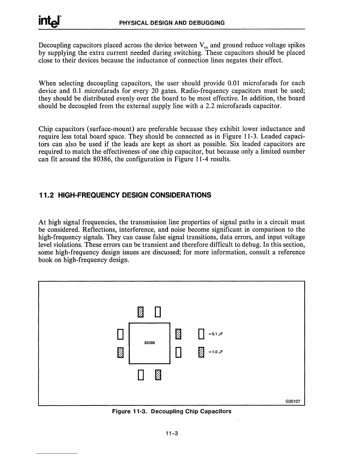
Chip capacitors (surface-mount) are preferable because they exhibit lower inductance and
require less total board space. They should be connected
as
in
Figure 11-3. Leaded capaci-
tors can also be used if the leads are kept
as
short
as
possible. Six leaded capacitors are
required to match the effectiveness of one chip capacitor, but because only a limited number
can fit around the 80386, the configuration
in
Figure 11-4 results.
11.2
HIGH-FREQUENCY DESIGN CONSIDERATIONS
At
high signal frequencies, the transmission line properties of signal paths
in
a circuit must
be considered. Reflections, interference, and noise become significant
in
comparison to the
high-frequency signals. They can cause false signal transitions, data errors, and input voltage
level violations. These errors can be transient and therefore difficult to debug. In this section,
some high-frequency design issues are discussed; for more information, consult a reference
book
on
high-frequency design.
D =0.1
pF
ill
=1.0pF
Figure
11-3.
Decoupling
Chip
Capacitors
11-3
G30107