PHYSICAL DESIGN AND DEBUGGING
11.1.2 Decoupling Capacitors
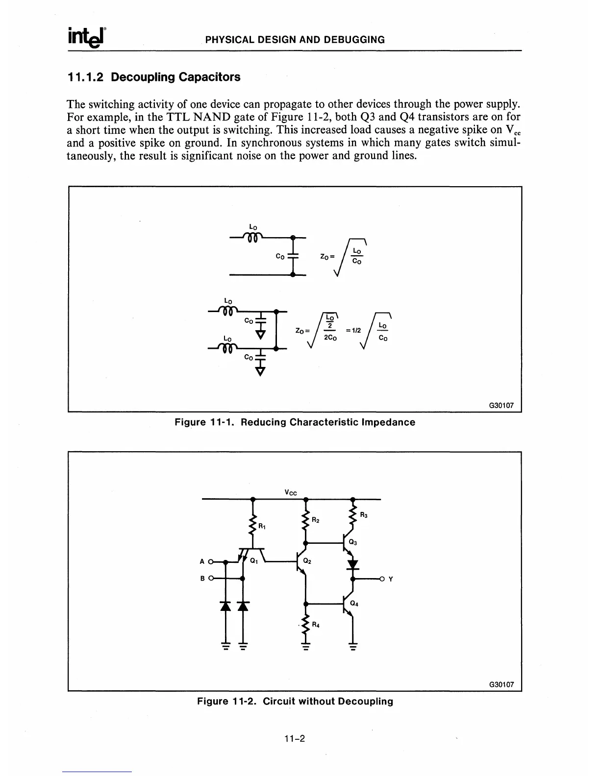
The switching activity of one device can propagate to other devices through the power supply.
For example, in the
TTL
NAND
gate of Figure 11-2, both
Q3
and Q4 transistors are
on
for
a short time when the output
is
switching. This increased load causes a negative spike on
Vee
and a positive spike on ground. In synchronous systems in which many gates switch simul-
taneously, the result
is
significant noise on the power and ground lines.
Zo=
-
F
o
Co
Lo
~
co~
fl
o
fi
2" Lo
Zo=
-
=112
-
2Co Co
G30107
Figure
11-1.
Reducing
Characteristic
Impedance
R3
A
B
o-+-
..
y
G30107
Figure
11-2.
Circuit
without
Decoupling
11-2
 Loading...


