DRAM PAL DESCRIPTIONS
Table
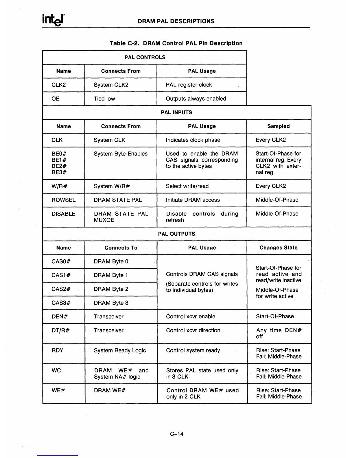
C-2. DRAM
Control
PAL Pin
Description
PAL
CONTROLS
Name Connects From
PAL
Usage
ClK2
System
ClK2
PAL register clock
OE
Tied low
Outputs always enabled
PAL
INPUTS
Name
Connects From
PAL
Usage
Sampled
ClK
System
ClK
Indicates clock phase Every CLK2
BEO#
System Byte-Enables Used to enable the
DRAM
Start-Of-Phase for
BE1#
CAS signals corresponding
internal reg. Every
BE2#
to the active bytes
ClK2
with exter-
BE3#
nal
reg
W/R#
System
W/R#
Select write/read Every
ClK2
ROWSEl
DRAM STATE PAL Initiate DRAM access Middle-Of-Phase
DISABLE
DRAM STATE PAL Disable
controls
during
Middle-Of-Phase
MUXOE
refresh
PAL
OUTPUTS
Name
Connects To
PAL
Usage Changes State
CASO#
DRAM Byte 0
Start-Of-Phase
for
CAS1#
DRAM Byte 1
Controls
DRAM
CAS signals read active and
(Separate controls for writes
read/write inactive
CAS2#
DRAM Byte 2
to individual bytes)
Middle-Of-Phase
for write active
CAS3#
DRAM Byte 3
DEN#
Transceiver Control xcvr enable
Start-Of-Phase
DT/R#
Transceiver
Control xcvr direction Any time
DEN#
off
RDY
System Ready
logic
Control system ready
Rise:
Start-Phase
Fall:
Middle-Phase
WC
DRAM
WE#
and
Stores
PAL state used only Rise: Start-Phase
System
NA#
logic
in
3-ClK
Fall:
Middle-Phase
WE#
DRAMWE#
Control
DRAM
WE#
used Rise: Start-Phase
only
in
2-ClK
Fall:
Middle-Phase
C-14

 Loading...


