LOCAL BUS INTERFACE
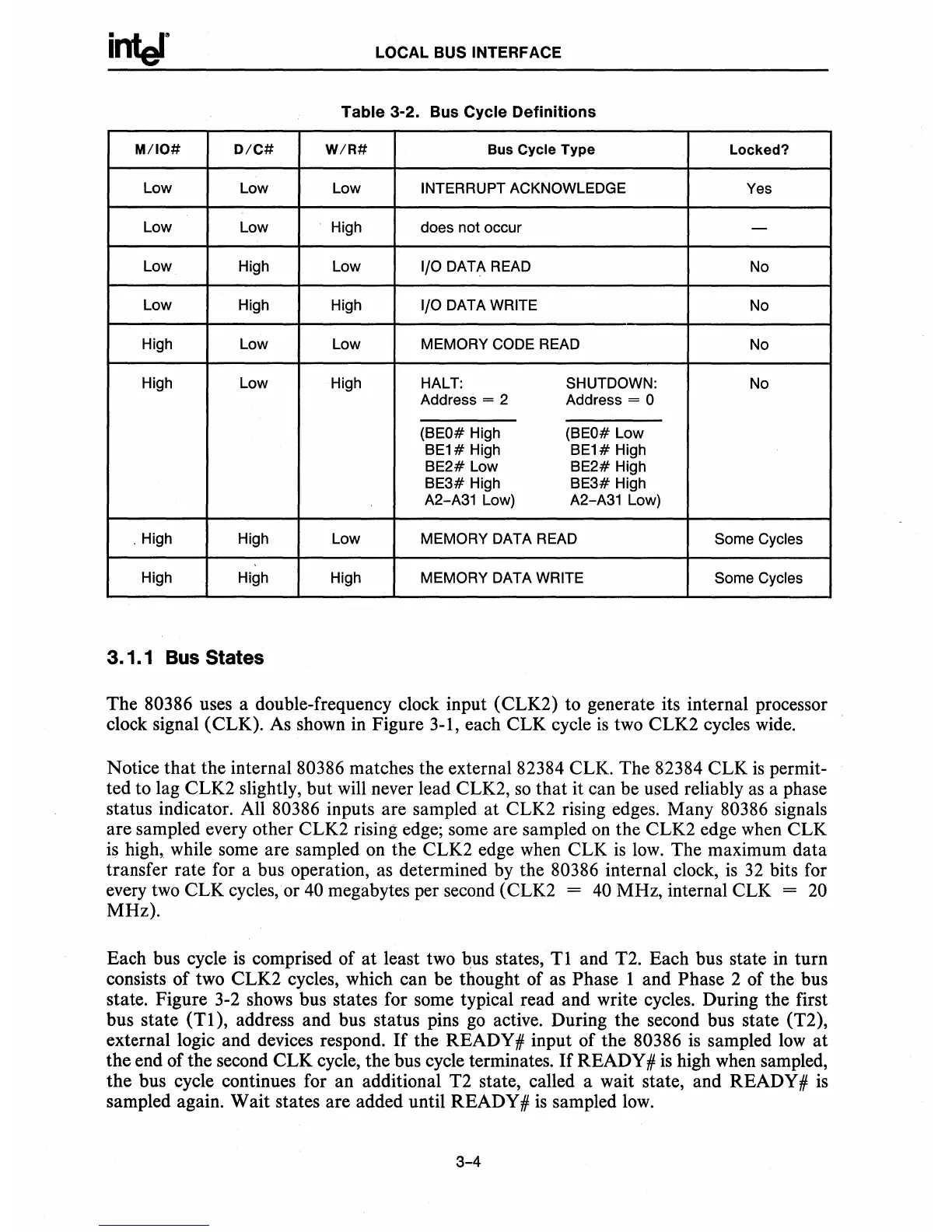
Table 3-2. Bus Cycle Definitions
M/IO#
D/C#
W/R#
Bus
Cycle
Type
Locked?
Low Low Low INTERRUPT ACKNOWLEDGE
Yes
Low Low High
does not occur
-
Low High Low
I/O DATA READ No
Low High High
I/O DATA WRITE No
High Low Low
MEMORY CODE READ
No
High Low High HALT:
SHUTDOWN: No
Address
= 2 Address = 0
(BEO# High (BEO# Low
BE1#
High
BE1#
High
BE2#
Low
BE2#
High
BE3#
High
BE3#
High
A2-A31 Low) A2-A31 Low)
. High
High
Low MEMORY DATA READ Some Cycles
High High
High
MEMORY DATA WRITE Some Cycles
3.
1.
1
Bus
States
The 80386 uses a double-frequency clock input (CLK2) to generate its internal processor
clock signal (CLK).
As
shown in Figure 3-1, each CLK cycle
is
two CLK2 cycles
wide.
Notice that the internal 80386 matches the external 82384 CLK. The 82384 CLK
is
permit-
ted to lag CLK2 slightly, but will never lead CLK2,
so
that it can be used reliably
as
a phase
status indicator. All
80386 inputs are sampled at CLK2 rising edges. Many 80386 signals
are sampled every other CLK2 rising edge; some are sampled
on
the CLK2 edge when CLK
is
high, while some are sampled on the CLK2 edge when CLK
is
low.
The maximum data
transfer rate for a bus operation,
as
determined
by
the 80386 internal clock,
is
32
bits for
every
two
CLK cycles, or
40
megabytes per second (CLK2 =
40
MHz, internal CLK =
20
MHz).
Each bus cycle
is
comprised of
at
least two bus states,
T1
and T2. Each bus state
in
turn
consists of two CLK2 cycles, which can be thought of
as
Phase 1 and Phase 2 of the bus
state. Figure 3-2 shows bus states for some typical read and write cycles. During the first
bus state
(Tl),
address and bus status pins
go
active. During the second bus state (T2),
external logic and devices respond.
If
the READY # input of the 80386
is
sampled
low
at
the end of the second CLK cycle, the bus cycle terminates.
If
READY #
is
high
when
sampled,
the bus cycle continues for an additional T2 state, called a wait state, and
READY #
is
sampled again. Wait states are added until READY#
is
sampled
low.
3-4