MEMORY INTERFACING
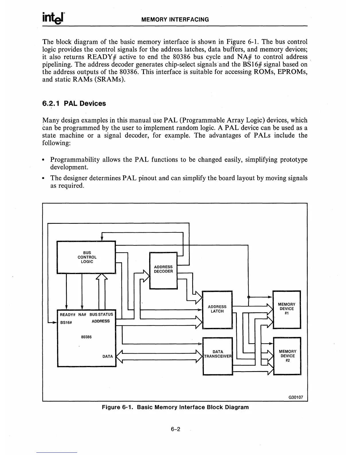
The block diagram of the basic memory interface
is
shown in Figure 6-1. The bus control
logic provides the control signals for the address latches, data buffers, and memory devices;
it also returns READY # active to end the 80386 bus cycle and
NA#
to control address
pipelining. The address decoder generates chip-select signals and the
BS16# signal based on
the address outputs of the
80386. This interface
is
suitable for accessing ROMs, EPROMs,
and static RAMs (SRAMs).
6.2.1
PAL
Devices
Many design examples in this manual use
PAL (Programmable Array Logic) devices, which
can be programmed
by
the user to implement random logic. A
PAL
device can be used
as
a
state machine or a signal decoder, for example. The advantages of
PALs include the
following:
• Programmability allows the
PAL
functions to
be
changed easily, simplifying prototype
development.
• The designer determines
PAL
pinout and can simplify the board layout by moving signals
as
required.
~
BUS
I--
CONTROL
I-
LOGIC
I-
ADDRESS
I--
--J....
DECODER
I---
'"
-V
I--
~
ADDRESS
I.
MEMORY
-
DEVICE
LATCH
#1
READY#
NA#
BUS STATUS
~
~
'-+-
BS16#
ADDRESS
--
v'
-vi
80386
L-
-
V'
~
DATA
'---
:;:
MEMORY
DATA
TRANSCEIVER
DEVICE
~
,/
-
#2
.,/
G30107
Figure
6-1. Basic
Memory
Interface
Block
Diagram
6-2