8XC196KC/8XC196KC20
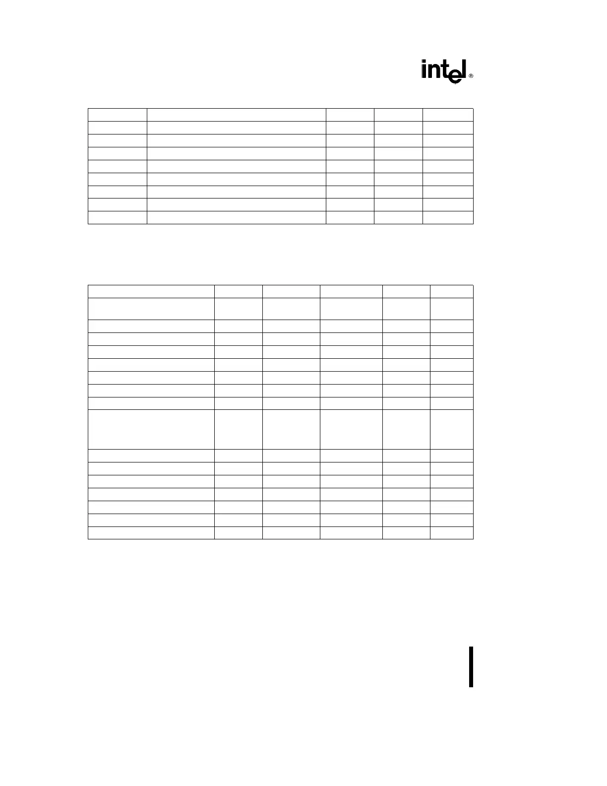
8-BIT MODE A/D OPERATING CONDITIONS
Symbol Description Min Max Units
T
A
Ambient Temperature Commercial Temp. 0
a
70
§
C
T
A
Ambient Temperature Extended Temp.
b
40
a
85
§
C
V
CC
Digital Supply Voltage 4.50 5.50 V
V
REF
Analog Supply Voltage 4.00 5.50 V
T
SAM
Sample Time 1.0 ms
(1)
T
CONV
Conversion Time 7 20 ms
(1)
F
OSC
Oscillator Frequency (8XC196KC) 8.0 16.0 MHz
F
OSC
Oscillator Frequency (8XC196KC20) 8.0 20.0 MHz
NOTE:
ANGND and V
SS
should nominally be at the same potential, 0.00V.
1. The value of AD
Ð
TIME is selected to meet these specifications.
8-BIT MODE A/D CHARACTERISTICS (Over Specified Operating Conditions)
Parameter Typical Minimum Maximum Units* Notes
Resolution 256 256 Levels
8 8 Bits
Absolute Error 0
g
1 LSBs
Full Scale Error
g
0.5 LSBs
Zero Offset Error
g
0.5 LSBs
Non-Linearity 0
g
1 LSBs
Differential Non-Linearity Error
l
b
1
a
1 LSBs
Channel-to-Channel Matching
g
1 LSBs
Repeatability
g
0.25 LSBs
Temperature Coefficients:
Offset 0.003 LSB/
§
C
Full Scale 0.003 LSB/
§
C
Differential Non-Linearity 0.003 LSB/
§
C
Off Isolation
b
60 dB 2, 3
Feedthrough
b
60 dB 2
V
CC
Power Supply Rejection
b
60 dB 2
Input Series Resistance 750 1.2K Xs4
Voltage on Analog Input Pin V
SS
b
0.5 V
REF
a
0.5 V 5, 6
DC Input Leakage 0
g
3.0 mA
Sampling Capacitor 3 pF
NOTES:
*An ‘‘LSB’’ as used here has a value of approximately 20 mV. (See Embedded Microcontrollers and Processors Handbook
for A/D glossary of terms).
1. These values are expected for most parts at 25
§
C but are not tested or guaranteed.
2. DC to 100 KHz.
3. Multiplexer Break-Before-Make is guaranteed.
4. Resistance from device pin, through internal MUX, to sample capacitor.
5. These values may be exceeded if pin current is limited to
g
2 mA.
6. Applying voltages beyond these specifications will degrade the accuracy of all channels being converted.
7. All conversions performed with processor in IDLE mode.
20
 Loading...
