Intel® Server Board S2600IP and Intel® Workstation Board W2600CR TPS List of Figures
Revision 1.1
Intel order number G34153-003
List of Figures
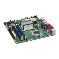
Figure 1. Intel
®
Server Board S2600IP ........................................................................................ 2
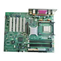
Figure 2. Intel
®
Workstation Board W2600CR ............................................................................. 2
Figure 3. Intel
®
Server Board S2600IP Major Components ......................................................... 6
Figure 4. Intel
®
Server Board S2600IP Rear I/O Layout .............................................................. 8
Figure 5. Intel
®
Workstation Board W2600CR Rear I/O Layout ................................................... 9
Figure 6. Mounting Hole Locations (1 of 2) ................................................................................ 10
Figure 7. Mounting Hole Locations (2 of 2) ................................................................................ 11
Figure 8. Major Connector Pin-1 Locations (1 of 3) ................................................................... 12
Figure 9. Major Connector Pin-1 Locations (2 of 3) ................................................................... 13
Figure 10. Major Connector Pin-1 Locations (3 of 3) ................................................................. 14
Figure 11. Primary Side Keep-out Zone .................................................................................... 16
Figure 12. Primary Side Card-Side Keep-out Zone ................................................................... 17
Figure 13. Second Side Keep-out Zone .................................................................................... 18
Figure 14. Intel
®
Server Board S2600IP Functional Block Diagram ........................................... 19
Figure 15. Intel
®
Workstation Board W2600CR Functional Block Diagram ................................ 20
Figure 16. Processor Socket Assembly ..................................................................................... 21
Figure 17. Processor Socket ILM .............................................................................................. 21
Figure 18. Integrated Memory Controller Functional Block Diagram .......................................... 26
Figure 19. DIMM Slot Layout ..................................................................................................... 30
Figure 20. External RJ45 NIC Port LED Definition .................................................................... 41
Figure 21. Supported I/O Module Options ................................................................................. 42
Figure 22. USB3.0 Discrete Host Controller Block Diagram ...................................................... 44
Figure 23. IEEE 1394b Discrete Host Controller Block Diagram ............................................... 45
Figure 24. Integrated BMC Hardware ........................................................................................ 51
Figure 25. High-level Fan Speed Control Process ..................................................................... 62
Figure 26. Setup Utility – TPM Configuration Screen ................................................................ 87
Figure 27. Video Connector Pin-out .......................................................................................... 98
Figure 28. Jumper Blocks (J1C3, J1F1, J1F2, J2F3, J2F2) ..................................................... 100
Figure 29. Stand by LED, Fan Fault LED and CPU Fault LED Location .................................. 106
Figure 30. DIMM Fault LED’s Location .................................................................................... 107
Figure 31. Location of System Status, System ID and POST Code Diagnostic LEDs.............. 108
Figure 32. Power Distribution Block Diagram .......................................................................... 114
Figure 33. Differential Noise test setup ................................................................................... 118
Figure 34. Output Voltage Timing ........................................................................................... 119
Figure 35. Turn On/Off Timing (Power Supply Signals) ........................................................... 120
Figure 36. POST Code Diagnostic LED Decoder .................................................................... 156