TEST 㞬ḱ㉔㉘㥉
10 11
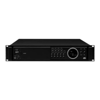
GGBLOCK DIAGRAM
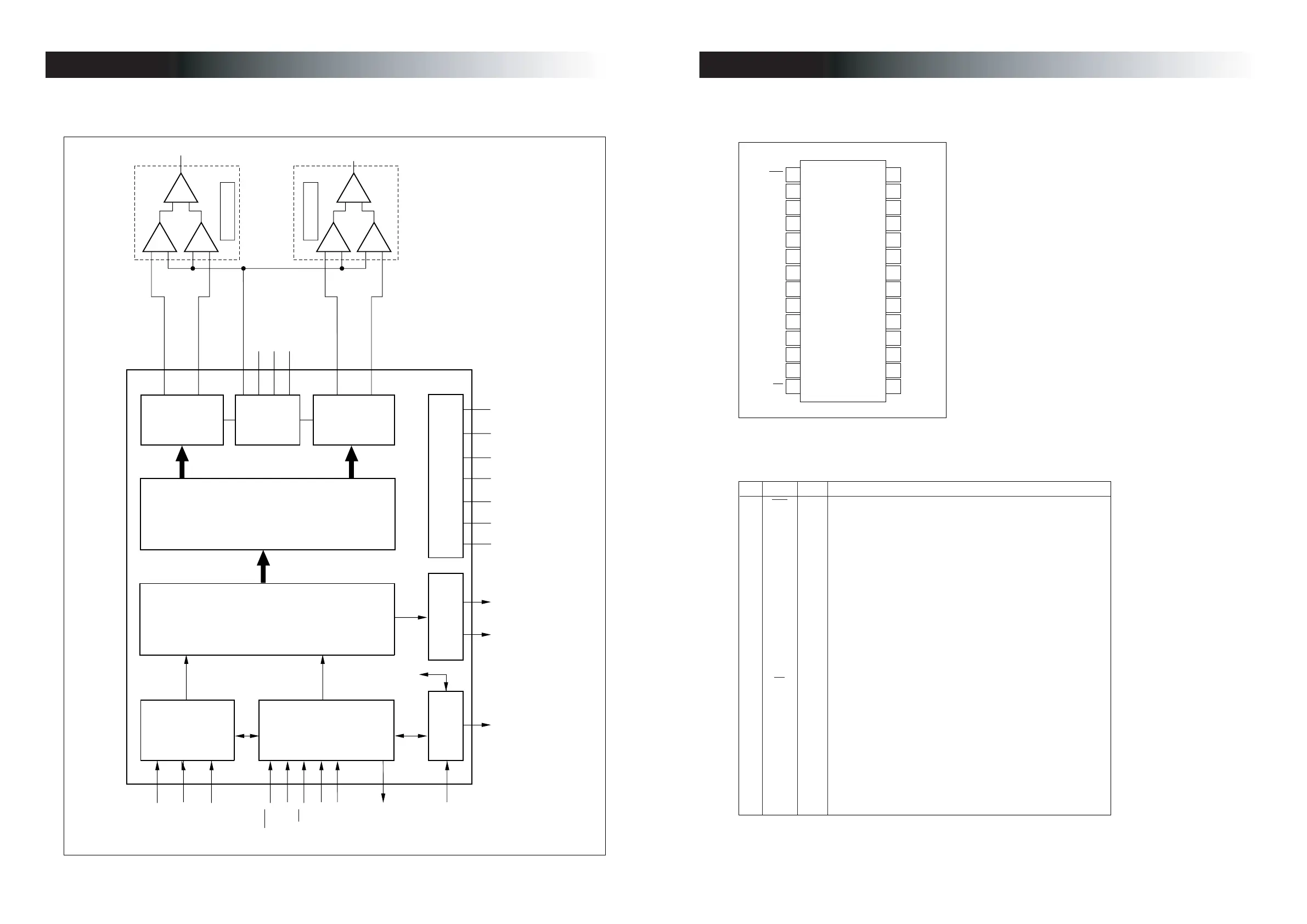
GPIN CONFIGURATION
GPIN ASSIGNMENT
RST
ZEROL
ZEROR
LRCK
DATA
BCK
SCKI
DGND
V
DD
SCKO
MDO
MDI
MC
CS
V
CC
3
AGND2
I
OUT
L–
I
OUT
L+
V
CC
2
V
CC
1
V
COM
3
I
REF
V
COM
2
V
COM
1
AGND1
I
OUT
R+
I
OUT
R–
MUTE
1
2
3
4
5
6
7
8
9
10
11
12
13
14
28
27
26
25
24
23
22
21
20
19
18
17
16
15
PCM1738
PIN NAME TYPE FUNCTION
1 RST IN Reset
(1)
2 ZEROL OUT Zero Flag for L-Channel.
3 ZEROR OUT Zero Flag for R-Channel.
4 LRCK IN Left/Right clock (f
S
) input for normal operation.
(1)
WDCK clock input in external DF mode. Connected to GND in DSD mode.
5 DATA IN Serial Audio data input for normal operation.
(1)
L-channel audio data input for external DF and DSD modes.
6BCK IN
Bit Clock. Input. Connected to GND for DSD mode.
(1)
7 SCKI IN System Clock Input for normal operation.
(1)
BCK (64f
S
) clock input for DSD mode.
8 DGND – Digital Ground
9V
DD
– Digital Supply, +3.3V
10 SCKO OUT System Clock Output
11 MDO OUT Serial data output for function control register.
(2)
12 MDI IN Serial data input for function control register.
(1)
13 MC IN Shift Clock for function control register.
(1)
14 CS IN Mode Control chip select and latch signal.
(1)
15 MUTE IN Analog output mute control for normal operation.
(1)
R-channel audio data input for external DF and DSD modes.
16 I
OUT
R – OUT R-Channel Analog Current Output –
17 I
OUT
R+ OUT R-Channel Analog Current Output +
18 AGND1 – Analog Ground
19 V
COM
1 – Internal Bias Decoupling Pin
20 V
COM
2 – Common Voltage for I/V
21 I
REF
– Output current reference bias pin. Connect 16k resistor to GND.
22 V
COM
3 – Internal Bias Decoupling Pin
23 V
CC
1 – Analog Supply, +5.0V
24 V
CC
2 – Analog Supply, +5.0V
25 I
OUT
L+ OUT L-Channel Analog Current Output +
26 I
OUT
L – OUT L-Channel Analog Current Output –
27 AGND2 – Analog Ground
28 V
CC
3 – Analog Power Supply, +5.0V
NOTES: (1) Schmitt-trigger input, 5V tolerant. (2) Tristate output.
Input
I/F
8x
Oversampling
Digital
Filter
and
Function
Control
Advanced
Segment
DAC
Modulator
BCK
System Clock
Manager
ZERO Detect
Power Supply
RST
MUTE
CS
MC
MDI
L
OREZ
RO
R
EZ
SCKI
System Clock
O
K
C
S
MDO
Function
Control
I/F
Current
Segment
DAC
Bias
and V
REF
Current
Segment
DAC
V
C
C
1
V
C
C
2
V
C
C
3
V
D
D
D
N
GD
1
D
N
GA
2DNG
A
LRCK
DATA
I
OUT
L+
I
OUT
L–
IV and Filter
I
OUT
R–
I
OUT
R+
V
COM
2
I
REF
V
COM
1
V
COM
3
IV and Filter