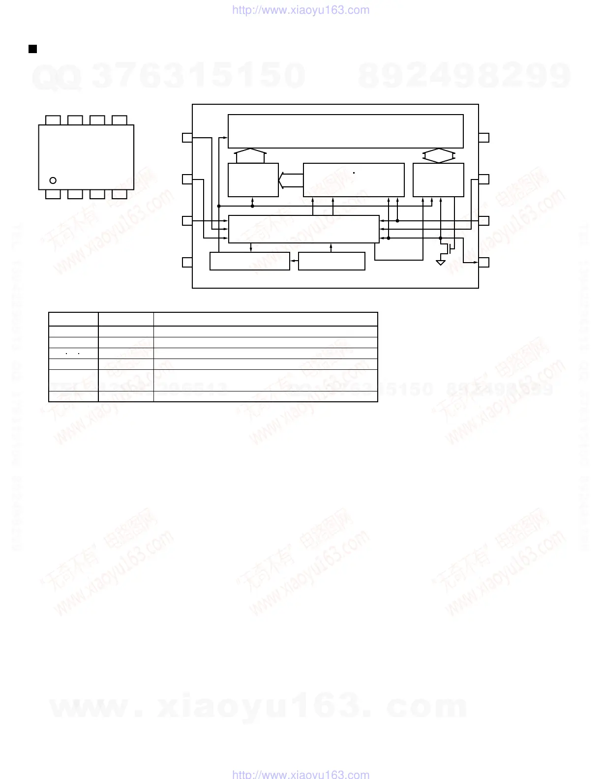
CH-X400/CH-X450
1-36
1A 0
2A 1
3A 2
4GND
8 VCC
7 TEST
6 SCL
5SDA
1,024bit EEPROM Array
7bit
8bit
7bit
Address
Decoder
Slave Word
Address Register
Data
Register
Control logic
High Voltage Gen.
Vcc level detect
START STOP
ACK
VCC TEST SCL SDA
BR24C01AF
A0 A1 A2 GND
BR24CO1AF(IC604):EP ROM
2.Block Diagrram1.Terminal Layout
3.Pin Function
(*)
An open drain output requires a pull-up resistor.
Symbol
VCC
GND
A1 A2 A3
SCL
SDA
TEST
I/O
-
-
I
I
I/O
I
Function
Puwer Supply
Ground(OV)
Slaves Address Set(Pin)
Serial Clock Input
Slaves and Word Address,Serial Data Input,
Serial Data Output(*)
Ground
w
w
w
.
x
i
a
o
y
u
1
6
3
.
c
o
m
Q
Q
3
7
6
3
1
5
1
5
0
9
9
2
8
9
4
2
9
8
T
E
L
1
3
9
4
2
2
9
6
5
1
3
9
9
2
8
9
4
2
9
8
0
5
1
5
1
3
6
7
3
Q
Q
TEL 13942296513 QQ 376315150 892498299
TEL 13942296513 QQ 376315150 892498299
http://www.xiaoyu163.com
http://www.xiaoyu163.com
 Loading...