DCBA
4
5
3
2
1 1
2
3
4
5
A DCB
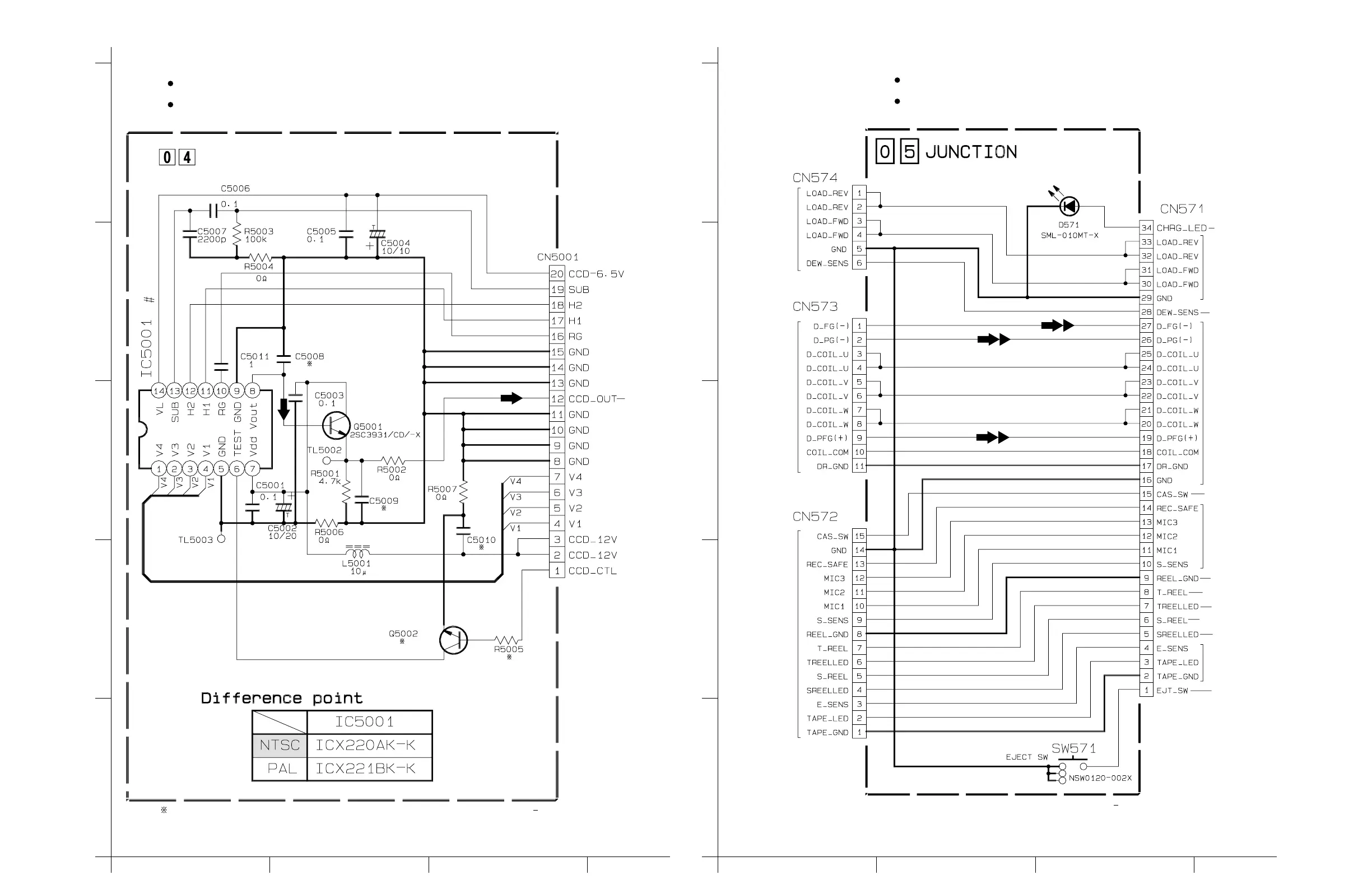
4.18 CCD SCHEMATIC DIAGRAM 4.19 JUNCTION SCHEMATIC DIAGRAM
4-37 4-38
this diagram
,
refer to "4.1 BOARD INTERCONNECTIONS".
For the destination of each signal and further line connections that are cut off from
The Parts Number
,
value and rated voltage etc. in the Schematic Diagram are for references only.
When replacing the parts
,
refer to the Parts List.
NOTES :
NOTES :
The Parts Number
,
value and rated voltage etc. in the Schematic Diagram are for references only.
For the destination of each signal and further line connections that are cut off from
When replacing the parts
,
refer to the Parts List.
this diagram
,
refer to "4.1 BOARD INTERCONNECTIONS".
CCD
NO WEAR
y40071001a rev0
CN107
TO TG/VDRV
TO CAM DSP
CN107
y40069001a rev0
DRUM MOTOR
TO
SENSOR
TO
LOADING MOTOR
TO
CN113
TO MDA
TO SYSCON CN113
TO VTR CPU CN113
CN113
TO MDA
TO SYSCON CN113
TO VTR CPU
CN113
TO MDA CN113
TO VTR CPU CN113
TO MDA CN113
TO VTR CPU CN113
TO MDA CN113
TO VTR CPU
CN113
TO SYSCON CN113
 Loading...