1-34 (No.49793)
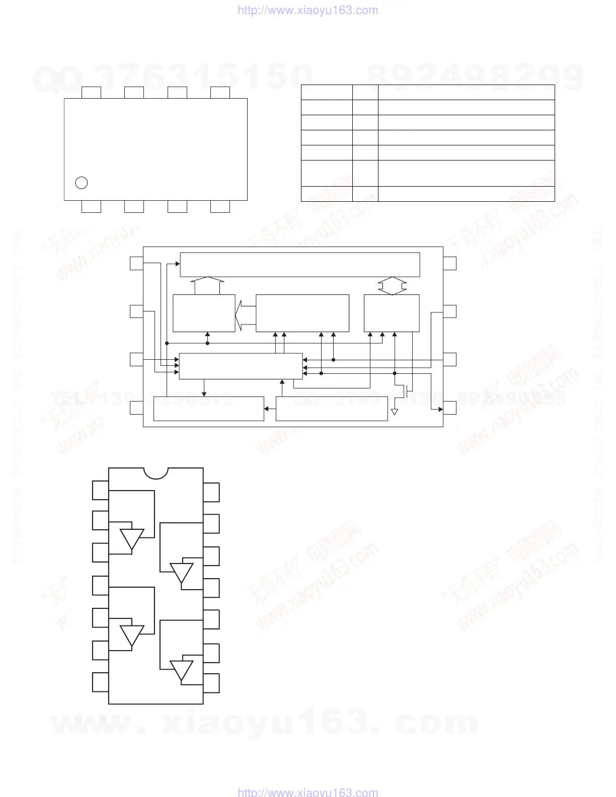
4.3 BR24C32F (IC703) : EEPROM
• Pin Layout
• Pin layout & Block diagram
• Pin function
4.4 HD74HC126FP (IC771) : Changer Control
SDASCLWP
BR24C32/F
VCC
GNDA2A1A0
PIN NAME I/O Function
VCC - Power Supply
GND - Ground (0V)
A0-A2 I Slave Address Set
SCL I Serial Clock Input
SDA I/O Slave and Word Address.
Serial Data Input$ Serial Data Output *1
WP I Write Protect Input
1
2
3
4
8
7
6
5
Vcc
WP
SCL
SD
A0
A1
A2
GND
32 Kbit EEPROM ARRAY
8bit
12bit
12bit
DATA
REGISTER
SLAVE WORD
ADDRESS REGISTER
ADDRESS
DECODER
START STOP
CONTROL LOGIC
VCC LEVEL DETECT
HIGH VOLTAGE GEN.
ACK
1
2
3
4
5
6
7
14
13
12
11
10
9
8
OE1
A1
Y1
OE2
A2
Y2
Vss
Vcc
OE4
A4
Y4
OE3
A3
Y3
HD74HC126
w
w
w
.
x
i
a
o
y
u
1
6
3
.
c
o
m
Q
Q
3
7
6
3
1
5
1
5
0
9
9
2
8
9
4
2
9
8
T
E
L
1
3
9
4
2
2
9
6
5
1
3
9
9
2
8
9
4
2
9
8
0
5
1
5
1
3
6
7
3
Q
Q
TEL 13942296513 QQ 376315150 892498299
TEL 13942296513 QQ 376315150 892498299
http://www.xiaoyu163.com
http://www.xiaoyu163.com
 Loading...