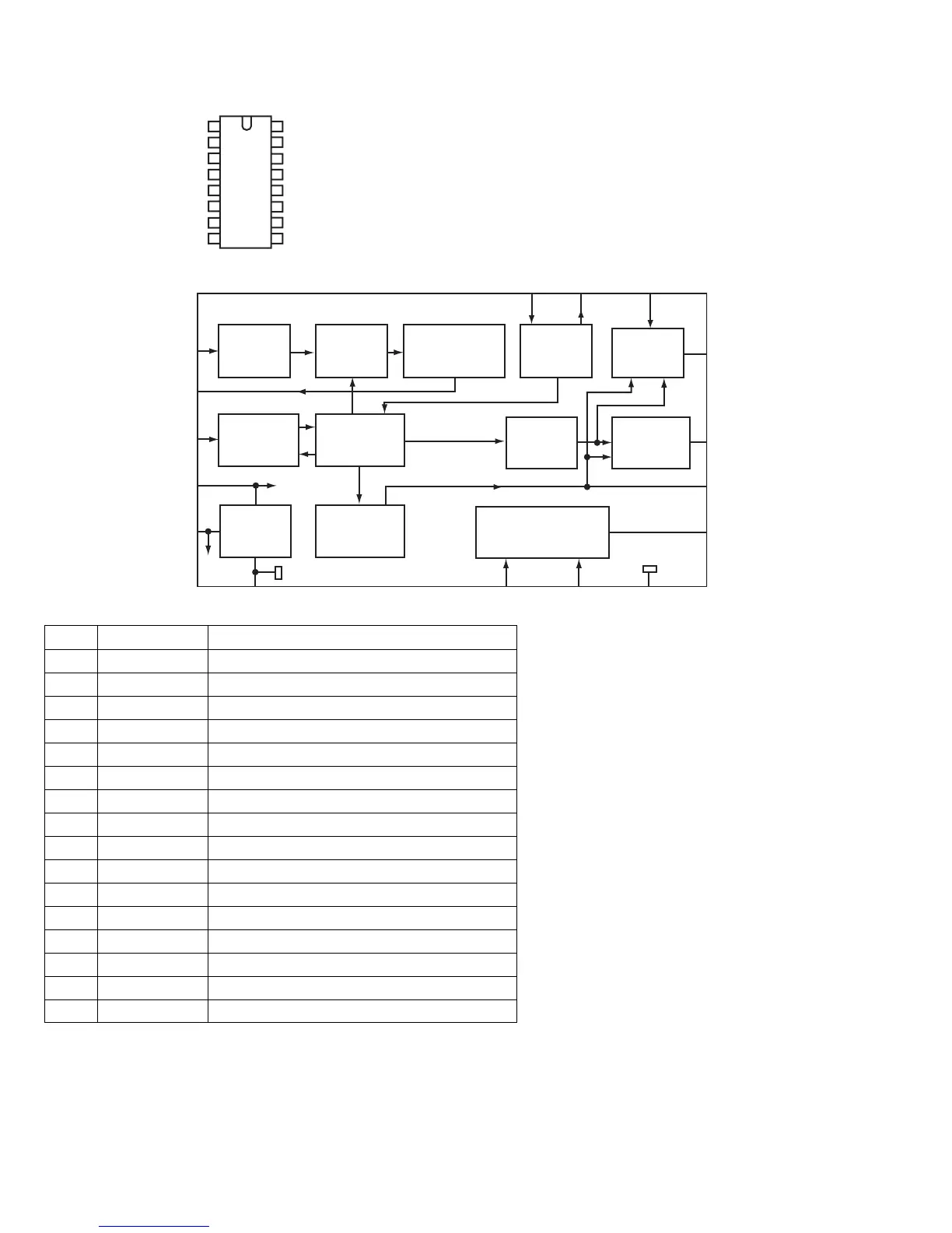
Pin No. Symbol Description
1 QUAL Quality indication output
2 DATA RDS data output
3 Vref Reference voltage output (0.5VDDA)
4 MUX Multiolex signal input
5 Vdd +5V supply voltage for analog part
6 GND Ground for analog part (0V)
7 CIN Sub carrier input to comparator
8 SCOUT Sub carrier output of reconstruction filter
9 MODE Oscillator mode / test control input
10 TEST Test enable input
11 GND Ground for digital part (0V)
12 Vdd +5V supply voltage for digital part
13 OSCI Oscillator input
14 OSCO Oscillator output
15 T57 57 kHz clock signal output
16 CLK RDS clock output
ANTI-
ALIASING
FILTER
CLOCKED
COMPARATOR
COSTAS LOOP
VARIABLE AND
FIXED DIVIDER
57 kHz
BAND PASS
(8th ORDER)
RECONSTRUCTION
FILTER
OSCILLATOR
AND
DIVIDER
BIPHASE
SYMBOL
DECODER
TEST LOGIC AND OUTPUT
SELECTOR SWITCH
CLOCK
REGERATION
AND SYNC
REFERENCE
VOLTAGE
DIFFERENTIAL
DECODER
QUALITY BIT
GENERATOR
8
4
7
5
VP1
3
6 11
15
15
2
1
121413
910
 Loading...