EasyManuals Logo

JVC SP-DW103 Service Manual

JVC SP-DW103
35 pages
To Next Page IconTo Next Page
To Previous Page IconTo Previous Page
Page #14 background imageLoading...
Page #14 background image
1-14 (No.22056)
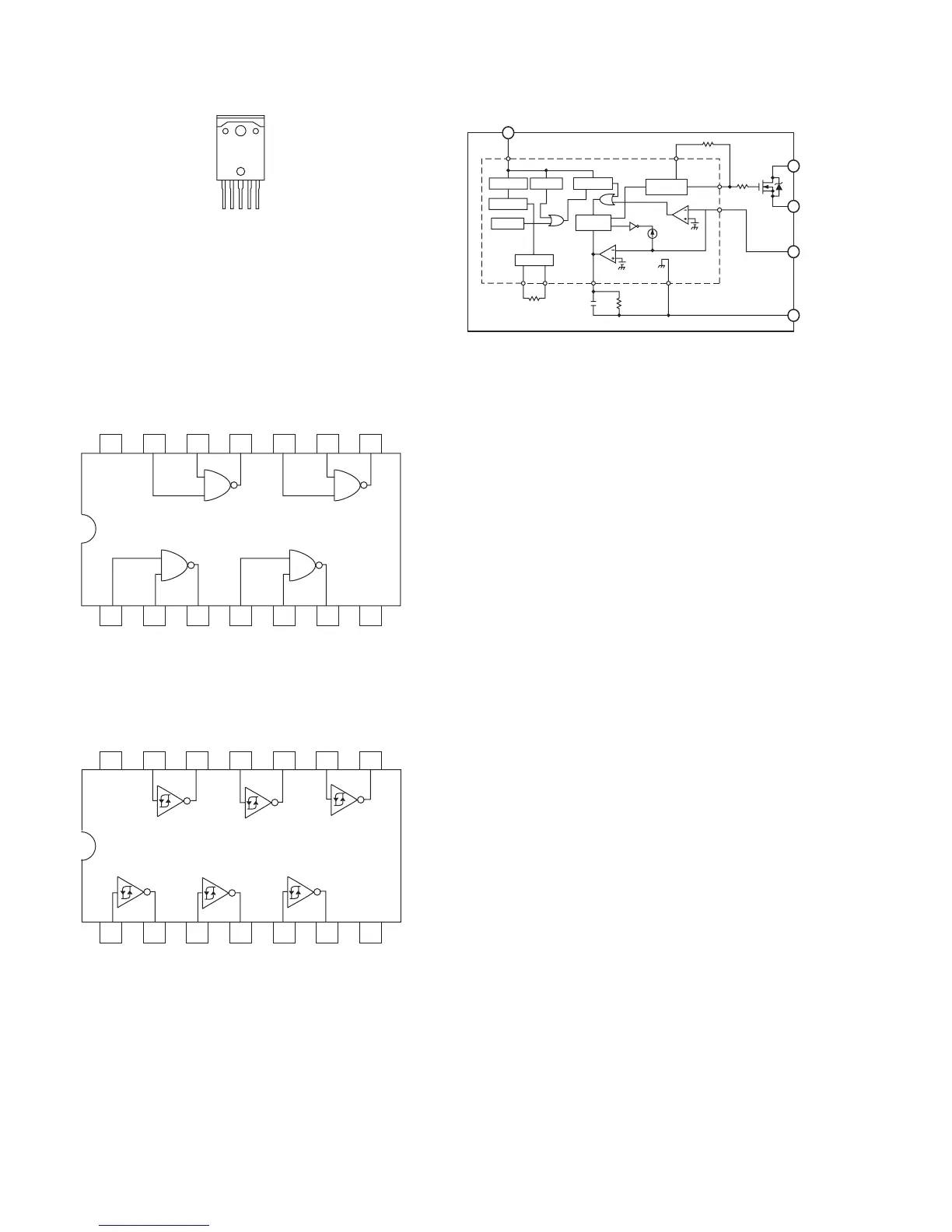
6.7 STR-F6676 (IC951) : Switching regulator
Pin Layout Block Diagram
6.8 TC74HC00AF-W (IC503) : Quad 2-input NAND gate
Pin layout & Block diagram
6.9 TC74HC14AF-X (IC504, IC571) : Hex Schmitt inverter
Pin layout & Block diagram
12 3 4
5
VIN
4
START
REG.
T.S.D
O.V.P
LATCH
O.S.C
DRIVE
Vth(1)
Comp.1
Vth(2)
Comp.2
GND
5
O.C.P./F.
B
1
S
2
D
3
R4
R3
R1C1
Iconst
R2
Rconst-Rconst+
14 13
12
11 10 9 8
7
6
543
2
1
1A 1B 1Y 2A 2B 2Y GND
Vcc 4B 4A 4Y 3B 3A 3Y
14 13
12
11 10 9 8
7
6
543
2
1
1A 1Y 2A 2Y 3A 3Y GND
Vcc 6A 6Y 5A 5Y 4A 4Y

Other manuals for JVC SP-DW103

Questions and Answers:

Question and Answer IconNeed help?

Do you have a question about the JVC SP-DW103 and is the answer not in the manual?

JVC SP-DW103 Specifications

General IconGeneral
BrandJVC
ModelSP-DW103
CategorySubwoofer
LanguageEnglish

Related product manuals