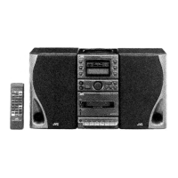
UX-A7DVD
(No.22013)1-45
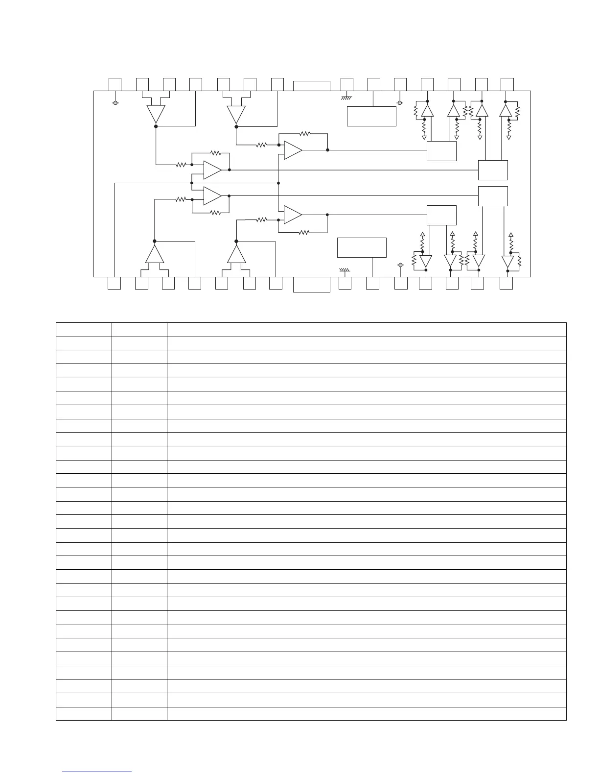
4.5 BA5983FM-X (IC201) : BTL driver
• Pin layout & Block diagram
• Pin function
28 27 26
25 24 23 22 21 20 19 18 17 16 15
21
3 4
5
6 7
89
10 11
12
13
14
+-+-
+-
+-
+-
+- +- +- +-
+-
+-
+-
Level
Sblft
STAND BY
C #4
STAND BY
C #1/2/3
VCC
Level
Sblft
Level
Sblft
Level
Sblft
VCC
VCC
+-
+- +-
+-
10k
10k
20k
10k
10k
10k
10k
10k
10k10k
10k
10k
10k
10k
10k
10k
10k
10k
10k
10k
10k
10k
10k
20k
10k
Pin No Symbol Function
1 BIAS IN NC
2 OPIN1(+) Output3 for motor
3 OPIN1(-) NC
4 OPOUT1 Output2 for motor
5OPIN2(+)NC
6 OPIN2(-) NC
7 OPOUT2 Output1 for motor
8GNDGND
9 STBY1 Positive input for hall input Amp1.
10 PowVCC1 Negative input for hall input Amp1.
11 VO2(-) Positive input for hall input Amp2.
12 VO2(+) Negative input for hall input Amp2.
13 VO1(-) Positive input for hall input Amp3.
14 VO1(+) Negative input for hall input Amp3.
15 VO4(-) Hall bias terminal
16 VO4(+) Brake Mode terminal
17 VO3(-) Capacitor connection pin for phase compensation
18 VO3(+) Short brake terminal
19 PowVCC2 3Phase synthesized FG signal output termnal
20 STBY2 Rotation detect signal output terminal
21 GND Torque control standard voltage input terminal
22 OPOUT3 Torque control voltage input terminal
23 OPIN3(-) START/STOP switch
24 OPIN3(+) FG signal output terminal
25 OPOUT4 Power supply for driver division
26 OPIN4(-) Gain switch
27 OPIN4(+) Power supply for driver division
28 PreVCC Resistance connection pin for output current sense
 Loading...