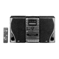
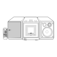
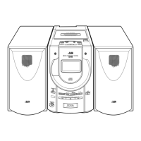
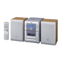
UX-A7DVD
1-46 (No.22013)
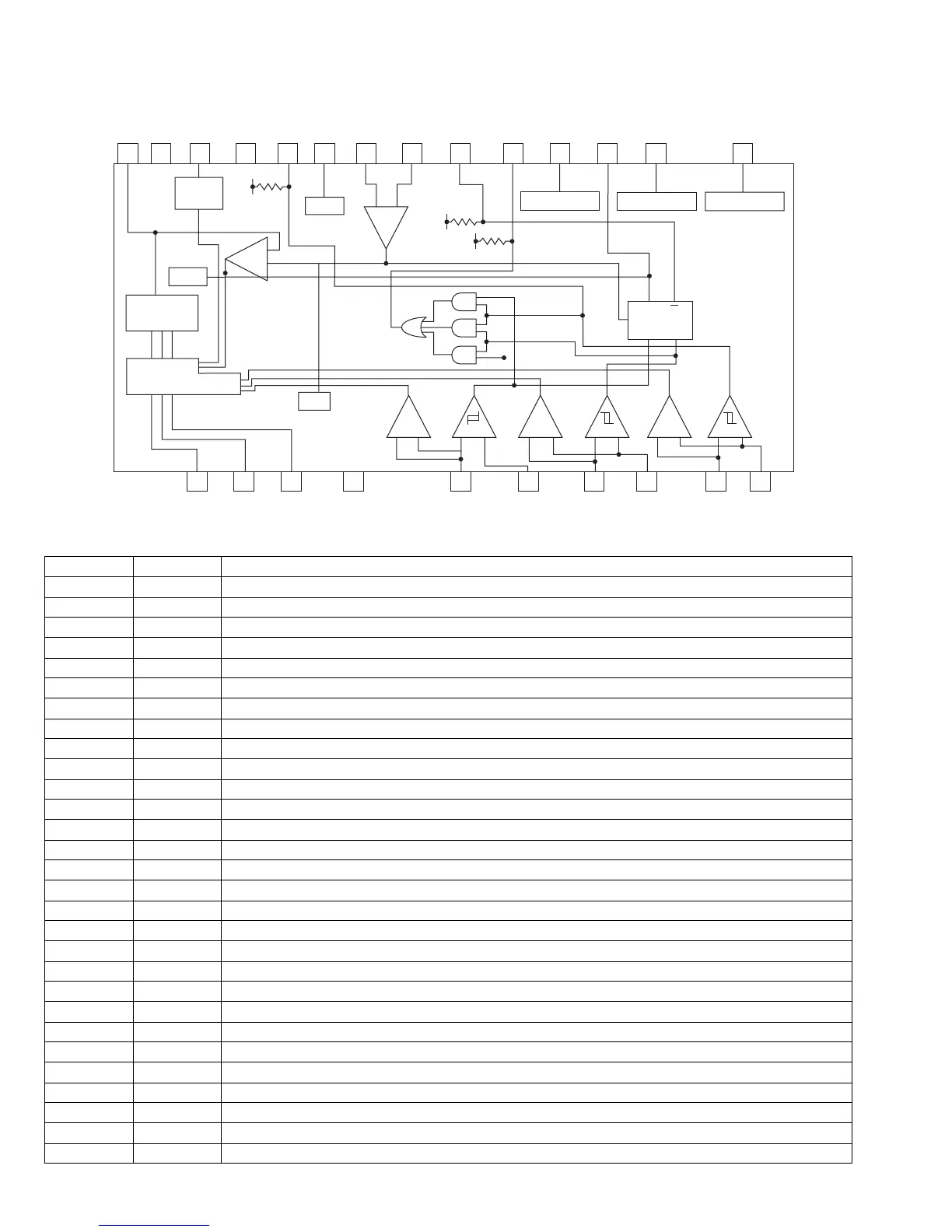
4.6 BA6664FM-X (IC251) : Motor driver
• Pin layout & Block diagram
• Pin function
28
RNF
A3 A2 A1 GND H1
+
H1
-
H2
+
H2
-
H3
+
H3
-
VM GSW VCC
2
4
7
8
910
11
12
13
14
27 26
25 24 23 22 21 20 19 18 17 16 15
+-
+-+-+-+-+-+-
+ -
DRIVER
GAIN
CONTROL
TL
HALL AMP
TSD
PS
TORQUE
VCC
VCC
SENSE AMP
GAIN
SWITCH
VCC
CURRENT
SENSE AMP
SHORT BRAKE BRAKE MODE
Hall Bias
R
Q Q
D
CK
VHBR
FG PS EC ECR FR FG2 SB CNF
Pin No. Symbol Function
1NCNC
2 A3 Output3 for motor
3NCNC
4 A3 Output2 for motor
5NCNC
6NCNC
7 A1 Output1 for motor
8GNDGND
9 H1+ Positive input for hall input Amp1.
10 H1- Negative input for hall input Amp1.
11 H2+ Positive input for hall input Amp2.
12 H2- Negative input for hall input Amp2.
13 H3+ Positive input for hall input Amp3.
14 H3- Negative input for hall input Amp3.
15 VH Hall bias terminal
16 BR Brake Mode terminal
17 CNF Capacitor connection pin for phase compensation
18 SB Short brake terminal
19 FG2 3Phase synthesized FG signal output termnal
20 FR Rotation detect signal output terminal
21 ECR Torque control standard voltage input terminal
22 EC Torque control voltage input terminal
23 PS START/STOP switch
24 FG FG signal output terminal
25 VCC Power supply for driver division
26 GSW Gain switch
27 VM Power supply for driver division
28 RNF Resistance connection pin for output current sense
FIN FIN GND
 Loading...