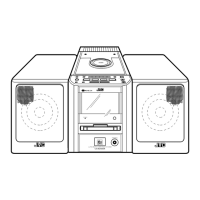
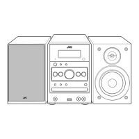
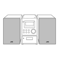
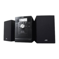
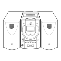
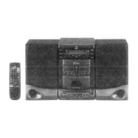
UX-M5R
1-31
18
19
20
21
22
23
24
25
26
27
28
29
30
SEB
VRO
RFRP
BTC
RFCT
PKC
RFRPIN
RFGO
GVSW
AGCIN
RFO
GND
RFN2
RFRP output circuit switching terminal
SEL level Bottom detection Peak detection
GND ON ON
Vcc OFF ON
Reference signal (VRO) output terminal
Track count signal output terminal
Time constant adjustment terminal for bottom detection
RFRP signal center level output terminal
Time constant adjustment terminal for peak detection
Input terminal for track count signal output amplifier
Output terminal for RF signal amplitude adjustment amplifier
Amplifier (AGC, FE, TE) gain switching terminal
GVSW Mode
GND CD-RW
Hiz Normal
Vcc Normal
Input terminal for RF signal amplitude adjustment amplifier
Output terminal RF signal amplifier
Ground terminal
Input terminal for RF signal amplifier
I
O
O
I
O
I
I
O
I
I
O
-
I
Pin No. Symbol I/O Function
IN2(M+)
Vcc
OUT2
NC
GND
Vs
OUT1
Vref
IN1(M+)
123456789
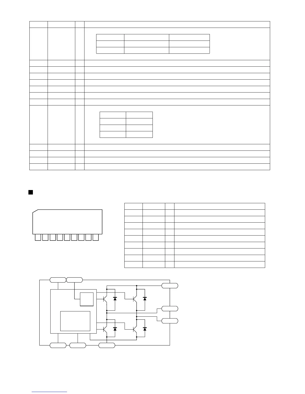
1.Terminal Layout
TA7291S (IC702) : Bridge driver
2.Pin function
Pin No. Symbol I/O Function
IN2(M-)
Vcc
OUT2
NC
GND
Vs
OUT1
Vref
IN1(M+)
1
2
3
4
5
6
7
8
9
Input terminal
Supply voltage terminal for logic
Output terminal
Not connect
Ground terminal
Supply voltage terminal for motor driver
Output terminal
Supply voltage terminal for control
Input terminal
I
-
O
-
-
-
O
-
I
REG
PROTECTOR
CIRCUIT
(TSD)
GND
OUT2
OUT1
6
3
7
Vs
28
Vcc Vref
91
IN1 IN2
5
3.Block diagram
 Loading...