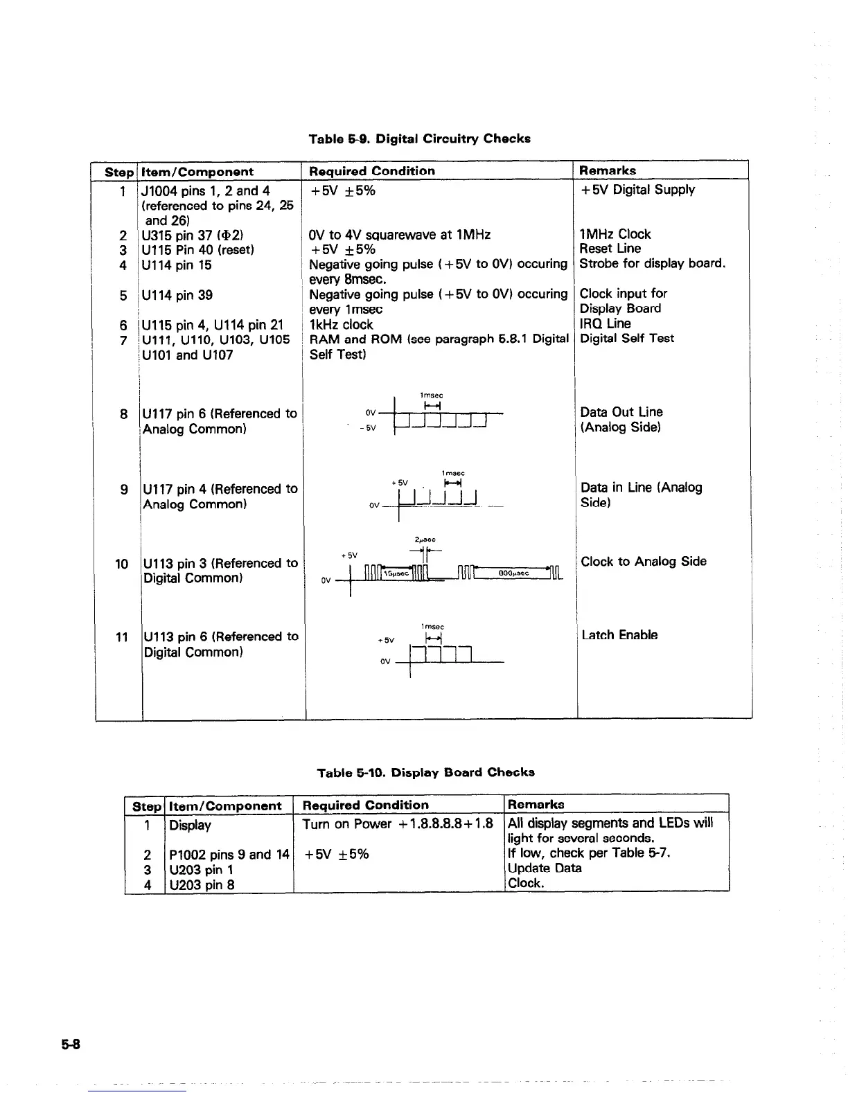
Table 9-9. Digital Circuitry Checks
Step Item/Component
1 J1004 pins 1, 2 and 4
(referenced to pins 24,
25
and 26)
2 U315 pin 37
(92)
3 U115 Pin 40 (reset)
4 U114 pin 15
5 iU114 pin 39
6 / U115 pin 4, U114 pin 21
7 IUlll, UllO, u103, u105
iUlO1 and U107
Required Condition
Remarks
+5v *5% +5V Digital Supply
OV to 4V squarewave at 1MHz
+5v 25%
Negative going pulse ( +5V to OV) occuring
every 8msec.
Negative going pulse ( +5V to OV) occuring
every lmsec
1 kHz clock
RAM and ROM (see paragraph 5.8.1 Digital
Self Test)
IMHz Clock
Reset Line
Strobe for display board.
Clock input for
Display Board
IRQ Line
Digital Self Test
/
8 /U117 pin 6 (Referenced to
/Analog Common)
Data Out Line
(Analog Side)
lrn?eC
+5v
0" /JLL
Z&&x
+ 5v
10 U113 pin 3 (Referenced to
It-
Digital Common)
ov
l-l
1msec
11 Ul13 pin 6 (Referenced to
Digital Common)
Data in Line (Analog
Side)
Clock to Analog Side
Latch Enable
Table 5-10. Display Board Checks
Step Item/Component
Required Condition Remarks
1 Display
Turn on Power + 1.8.8.8.8+ 1.8
All display segments and LEDs will
light for several seconds.
2 P1002 pins 9 and 14 + 5V +5%
If low, check per Table 5-7.
3 U203 pin 1
Update Data
4 U203 pin 8
Clock.
5-8