TH-K20A/K20E
8
FM IC: TA31136FNG (TX-RX unit IC200)
Pin No. Port Name I/O Function
1 OSCIN I 2nd Local oscillator input
2 OSCOUT O 2nd Local oscillator output
3 MIXOUT O MIX output
4 VCC - Power supply (5.0V)
5 IFIN I 2nd IF input and decoupling
6 DEC - 2nd IF input and decoupling
7 FILOUT O INVERTER AMP output
8 FILIN I INVERTER AMP input
9 AFOUT O Demodulate signal output
10 QUAD I
Phase shift signal input of FM
demodulator
11 IFOUT O Output terminal of IF AMP
12 RSSI O This terminal outputs DC
13 NOISEDET - level according to input (Not use)
14 NOISEREC - signal level to IF AMP
15 GND - Ground
16 MIXIN I 1st IF signal input
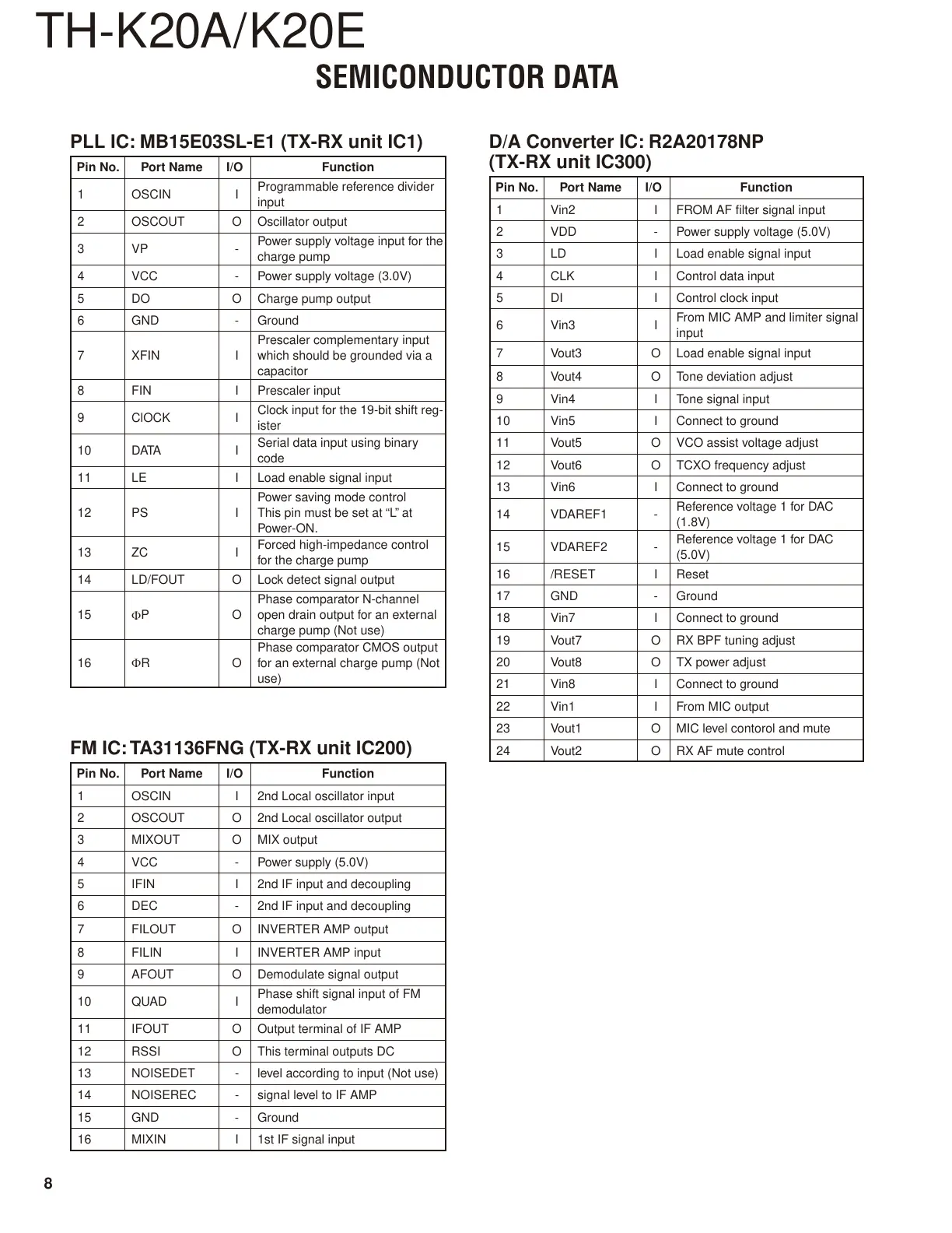
D/A Converter IC: R2A20178NP
(TX-RX unit IC300)
Pin No. Port Name I/O Function
1 Vin2 I FROM AF fi lter signal input
2 VDD - Power supply voltage (5.0V)
3 LD I Load enable signal input
4 CLK I Control data input
5 DI I Control clock input
6 Vin3 I
From MIC AMP and limiter signal
input
7 Vout3 O Load enable signal input
8 Vout4 O Tone deviation adjust
9 Vin4 I Tone signal input
10 Vin5 I Connect to ground
11 Vout5 O VCO assist voltage adjust
12 Vout6 O TCXO frequency adjust
13 Vin6 I Connect to ground
14 VDAREF1 -
Reference voltage 1 for DAC
(1.8V)
15 VDAREF2 -
Reference voltage 1 for DAC
(5.0V)
16 /RESET I Reset
17 GND - Ground
18 Vin7 I Connect to ground
19 Vout7 O RX BPF tuning adjust
20 Vout8 O TX power adjust
21 Vin8 I Connect to ground
22 Vin1 I From MIC output
23 Vout1 O MIC level contorol and mute
24 Vout2 O RX AF mute control
PLL IC: MB15E03SL-E1 (TX-RX unit IC1)
Pin No. Port Name I/O Function
1 OSCIN I
Programmable reference divider
input
2 OSCOUT O Oscillator output
3VP -
Power supply voltage input for the
charge pump
4 VCC - Power supply voltage (3.0V)
5 DO O Charge pump output
6 GND - Ground
7 XFIN I
Prescaler complementary input
which should be grounded via a
capacitor
8 FIN I Prescaler input
9 ClOCK I
Clock input for the 19-bit shift reg-
ister
10 DATA I
Serial data input using binary
code
11 LE I Load enable signal input
12 PS I
Power saving mode control
This pin must be set at “L” at
Power-ON.
13 ZC I
Forced high-impedance control
for the charge pump
14 LD/FOUT O Lock detect signal output
15
PO
Phase comparator N-channel
open drain output for an external
charge pump (Not use)
16
RO
Phase comparator CMOS output
for an external charge pump (Not
use)
SEMICONDUCTOR DATA
 Loading...