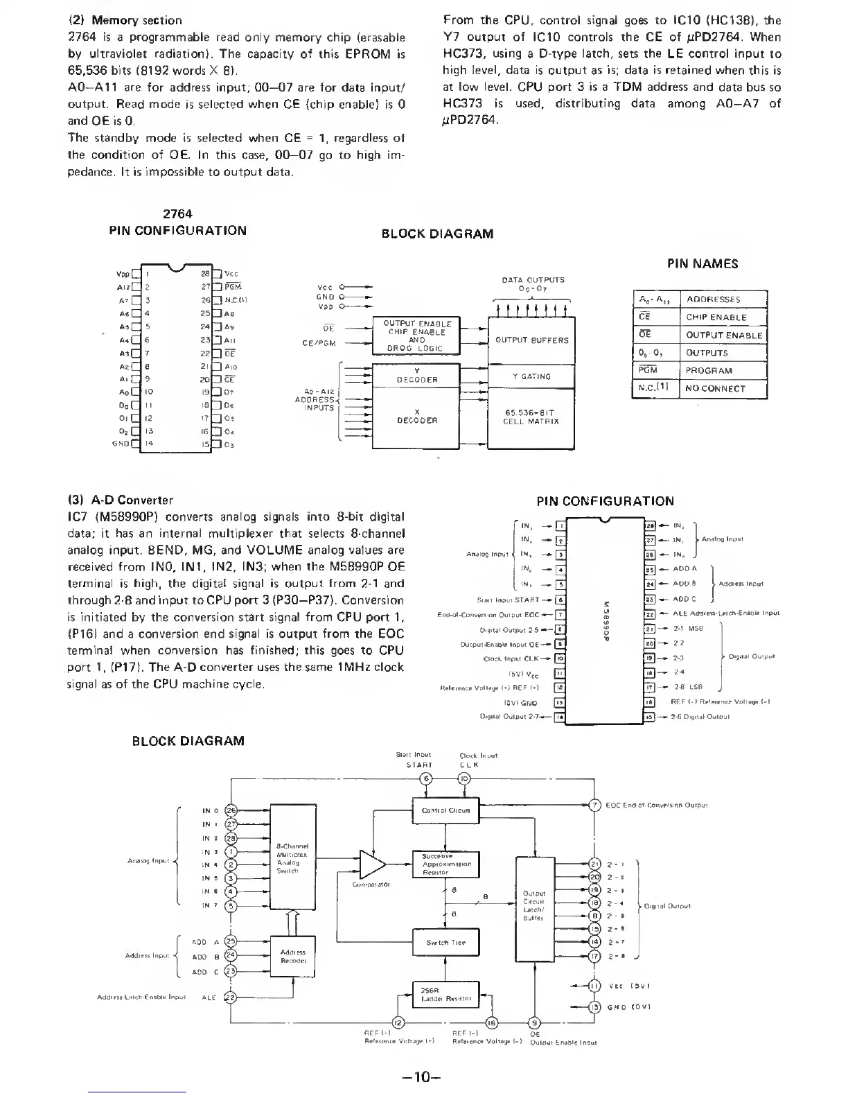
(2)
Memory section
2764 is
a
programmable
read only memory chip (erasable
by ultraviolet radiation). The capacity of this EPROM
is
65,536 bits (8192 words X
8).
AO—All are for address input;
00—07
are for
data
input/
output. Read mode
is
selected when
CE
(chip enable)
is 0
and OE
is 0.
The standby mode is selected when CE
=
1,
regardless of
the condition of OE. In this case, 00—07 go to high im-
pedance.
It
is Impossible
to
output
data.
From
the CPU, control signal
goes to
ICIO {HC138}, the
Y7 output of ICIO controls the CE
of /iPD2764. When
HC373, using
a D-type
latch,
sets
the
LE control input to
high level, data is output as is; data
is
retained when this
is
at low level. CPU port 3 is a TDM address and
data bus so
HC373 is used,
distributing
data among AO—A7 of
^PD2764.
2764
PIN CONFIGURATION
BLOCK
DIAGRAM
PIN NAMES
DATA OUTPUTS
(3)
A-D Converter
IC7
(M58990P) converts analog signals into 8-bit digital
data; it
has an internal multiplexer that
selects 8-channel
analog input. BEND, MG, and VOLUME analog
values
are
received
from
INO, INI,
IN2, IN3; when the M58990P OE
terminal
is
high, the digital signal is output from
2-1
and
through
2-8
and input
to
CPU port
3
(P30—
P37).
Conversion
is initiated by the conversion
start signal from
CPU port
1,
(P16) and a conversion end
signal
is output
from the
EOC
terminal when conversion has finished; this goes to CPU
port
1
,
(PI
7).
The A-D converter uses the same IMHz clock
signal as of the CPU
machine cycle.
PIN CONFIGURATION
Andlofl
Inptii
INi
.
ST4ri lnou<
START
•
Cn<>of>Conv^iof) Ouipvit £OC«
0<9it4il
Outpvt 3 S
*
Output-EnAOl0 Input
0€
~
Clock
Input CLK-
iSV)
Ktl*r«r>c«
Voiiagt
('J
REF
(*)
lOV)
GNO
0»giial
OuUNi
2*7^
I*-,
-c
«)•*“
1'*.
'
IN.
—[7
IN,
IN,
^[T
«]
•-
‘N.
.
IN.
-E ^
— ADDA
'[I
•Ci
-n.
•d
•
Go
E
E
E
•E
El-
E'
E-
«]-
3-
E-
3-
3
3-
•
ADO B
^
AddriM Input
-
AOOC
'
ALE
Addrto
LATcn>€rt«i>l0 Input
• 2'^
Mse
22
.
2.3
^
Oi9»W OulpuT
• 2-4
'
2-e Lse
REF
<•)
RiUrenc* Voliagt
<*l
2
6
D*9kUl Output
BLOCK DIAGRAM
Aratos
Input V
Addreu Input
iN 9
IN
*
IN i
IN
•
IN
7
AOO
A
ADO
8
Addtttt-LAIch-Cnablt Input
ALE
Start Input
START
Clock
Input
CL
K
REF l-l
Rr**ioncB Voltagr
(-1
EOC
Entf.ot.Conv«rpon Output
2
•
I
2-1
2
-*
2-3
2-y
2-3
>
Otpital
Output
Vcc ISVI
GND
(OV)
HEE(-1
OE
Rdettno Voltage (-)
Output-Enapie
Input
-
10
-
 Loading...