S94P01C -e1
19
5.1.3 P3 - Controller Interface
P3 is a 50-pin SCSI connector for interfacing to the front-end of the controllers. It is
strongly recommended that you use OEM cables to aid in satisfying CE requirements.
Contact your Lenze representative for assistance.
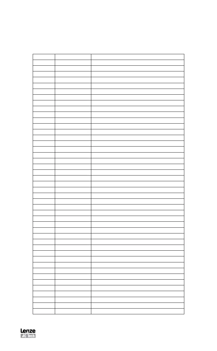
P3 Pin Assignments (Controller Interface)
Pin Name Function
1 MA+ Master Encoder A+ / Step+ input
(2)
2 MA- Master Encoder A- / Step- input
(2)
3 MB+ Master Encoder B+ / Direction+ input
(2)
4 MB- Master Encoder B- / Direction- input
(2)
5 GND Drive Logic Common
6 5+ +5V output (max 100mA)
7 BA+ Buffered Encoder Output: Channel A+
(1)
8 BA- Buffered Encoder Output: Channel A-
(1)
9 BB+ Buffered Encoder Output: Channel B+
(1)
10 BB- Buffered Encoder Output: Channel B-
(1)
11 BZ+ Buffered Encoder Output: Channel Z+
(1)
12 BZ- Buffered Encoder Output: Channel Z-
(1)
13-19 Empty
20 AIN2+ Positive (+) of Analog signal input
21 AIN2- Negative (-) of Analog signal input
22 ACOM Analog common
23 AO Analog output (max 10 mA)
24 AIN1+ Positive (+) of Analog signal input
25 AIN1 - Negative (-) of Analog signal input
26 IN_A_COM Digital input group ACOM terminal
(3)
27 IN_A1 Digital input A1
28 IN_A2 Digital input A2
29 IN_A3 Digital input A3
(3)
30 IN_A4 Digital input A4
31 IN_B_COM Digital input group BCOM terminal
32 IN_B1 Digital input B1
33 IN_B2 Digital input B2
34 IN_B3 Digital input B3
35 IN_B4 Digital input B4
36 IN_C_COM Digital input group CCOM terminal
37 IN_C1 Digital input C1
38 IN_C2 Digital input C2
39 IN_C3 Digital input C3
40 IN_C4 Digital input C4
41 RDY+ Ready output Collector
42 RDY- Ready output Emitter
43 OUT1-C Programmable output #1 Collector
44 OUT1-E Programmable output #1 Emitter
45 OUT2-C Programmable output #2 Collector
46 OUT2-E Programmable output #2 Emitter
47 OUT3-C Programmable output #3 Collector
48 OUT3-E Programmable output #3 Emitter
49 OUT4-C Programmable output #4 Collector
50 OUT4-E Programmable output #4 Emitter
(1)
See Note 1, Section 5.1.7 - Connector and Wiring Notes
(2)
See Note 2, Section 5.1.7 - Connector and Wiring Notes
3)
See Note 3, Section 5.1.7 - Connector and Wiring Notes
 Loading...