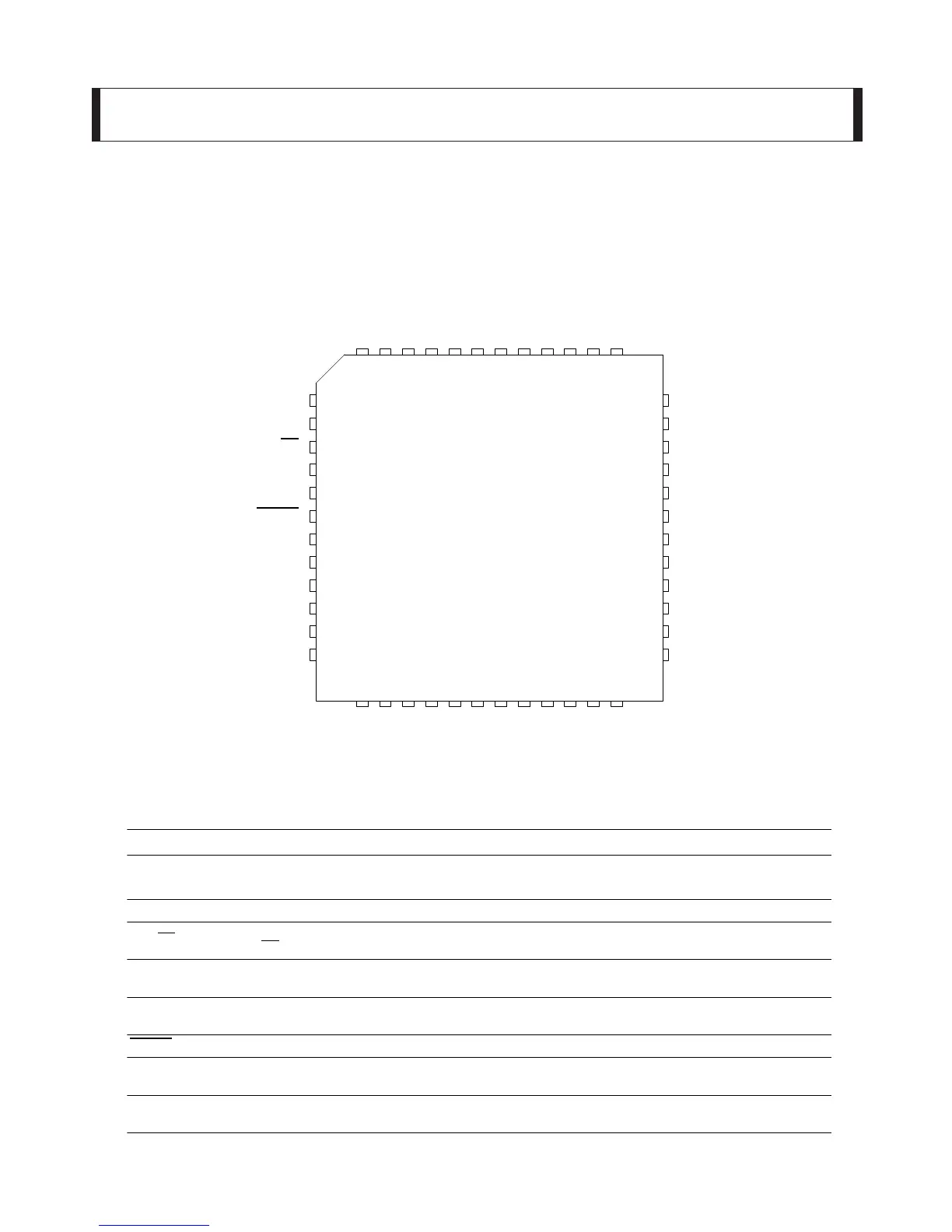
Pin Name # Pin Description
SDA/CDOUT 1
Serial Control Data (Input/Output) - SDA is a data I/O in I≤C
Æ
Mode. CDOUT is the output data line for
the control port interface in SPI
TM
Mode.
SCL/CCLK 2 Serial Control Port Clock (Input) - Serial clock for the serial control port.
AD0/CS
3
Address Bit 0 (I≤C) / Control Port Chip Select (SPI) (Input) - AD0 is a chip address pin in I≤C Mode;
CS is the chip-select signal for SPI format.
AD1/CDIN 4
Address Bit 1 (I≤C) / Serial Control Data Input (SPI) (Input) - AD1 is a chip address pin in I≤C Mode;
CDIN is the input data line for the control port interface in SPI Mode.
VLC 5
Control Port Power (Input) - Determines the required signal level for the control port interface. Refer
to the Recommended Operating Conditions for appropriate voltages.
RESET 6 Reset (Input) - The device enters a low-power mode when this pin is driven low.
AIN3A
AIN3B
7
8
Stereo Analog Input 3 (Input) - The full-scale level is specified in the ADC Analog Characteristics
specification table.
AIN2A
AIN2B
9
10
Stereo Analog Input 2 (Input) - The full-scale level is specified in the ADC Analog Characteristics
specification table.
 Loading...