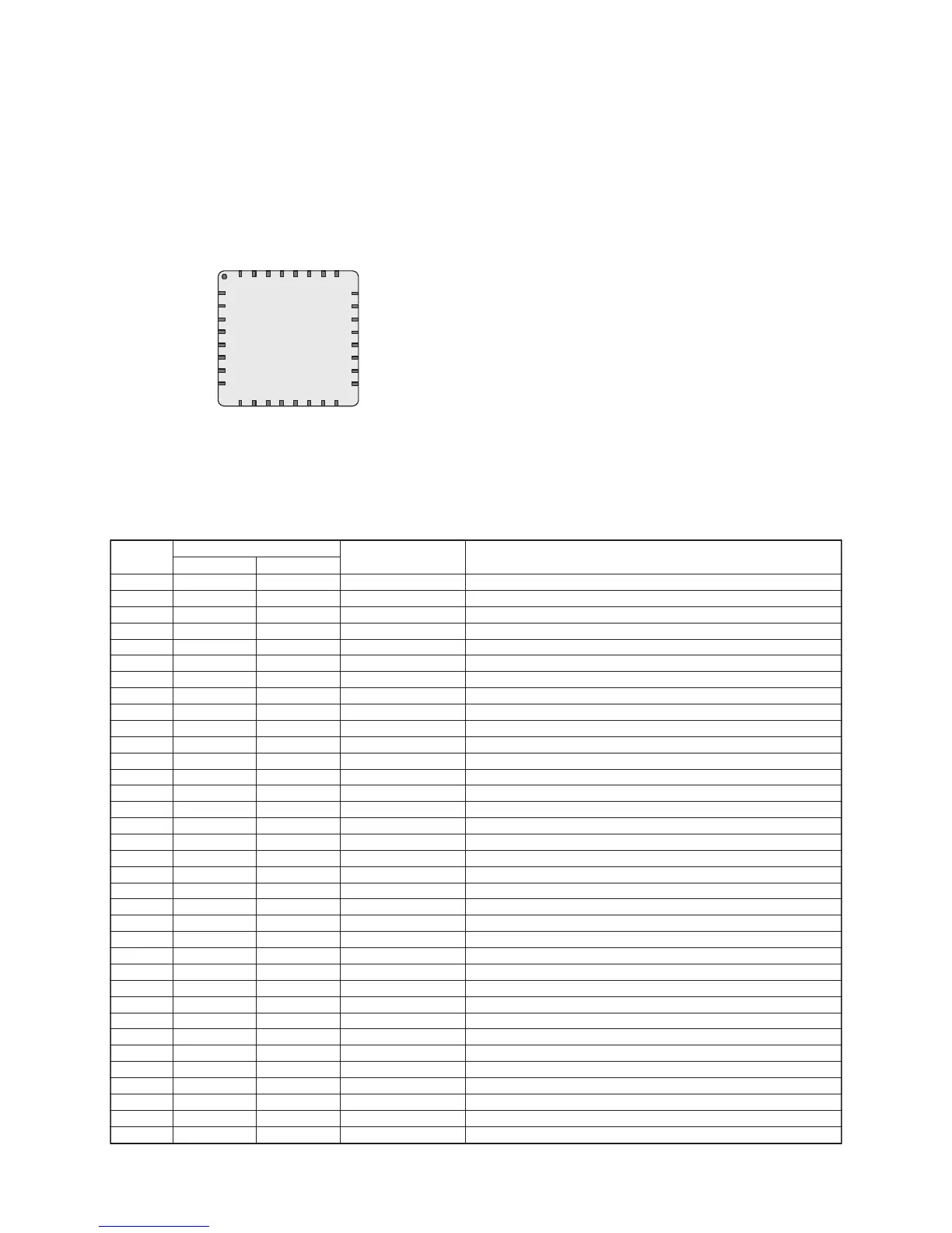
A, I, M, P0[1]
M, P2[7]
M, P2[5]
M, P2[3]
M, P2[1]
M, P3[3]
QFN
(Top View )
9
10
11
12
13
14
15
16
1
2
3
4
5
6
7
8
24
23
22
21
20
19
18
17
32
31
30
29
28
27
26
25
Vss
P0[3], A, I, M
P0[7], A, I, M
Vdd
P0[6], A, I, M
P0[4], A, I, M
P0[2], A, I, M
M, P3[1]
M, I2 C S C L , P1 [ 7 ]
P0 [0 ] , A , I, M
P2 [6 ] , M
P3 [0 ] , M
XRES
M, I2C SDA, P1[5]
M, P1[3]
M, I2C SCL, P1[1]
Vss
M, I2C SDA, P1[0]
M, P1[2]
M, EXT CLK, P1[4]
M, P1[6]
P2 [4 ] , M
P2 [2 ] , M
P2 [0 ] , M
P3 [2 ] , M
P0[5], A, I, M
SYMBOL DescriptionPin No.
Type
Digital Analog
1 IO I, M P0[1] Analog column mux input, integrating input.
2 IO M P2[7]
3 IO M P2[5]
4 IO M P2[3]
5 IO M P2[1]
6 IO M P3[3] In CY8C21434 part.
6 Power SMP Switch Mode Pump (SMP) connection to required external
components in CY8C21634 part.
7 IO M P3[1] In CY8C21434 part.
7 Power Vss Ground connection in CY8C21634 part.
8 IO M P1[7] I2C Serial Clock (SCL).
9 IO M P1[5] I2C Serial Data (SDA).
10 IO M P1[3]
11 IO M P1[1] I2C Serial Clock (SCL), ISSP-SCLK*.
12 Power Vss Ground connection.
13 IO M P1[0] I2C Serial Data (SDA), ISSP-SDATA*.
14 IO M P1[2]
15 IO M P1[4] Optional External Clock Input (EXTCLK).
16 IO M P1[6]
17 Input XRES Active high external reset with internal pull down.
18 IO M P3[0]
19 IO M P3[2]
20 IO M P2[0]
21 IO M P2[2]
22 IO M P2[4]
23 IO M P2[6]
24 IO I, M P0[0] Analog column mux input.
25 IO I, M P0[2] Analog column mux input.
26 IO I, M P0[4] Analog column mux input.
27 IO I, M P0[6] Analog column mux input.
28 Power Vdd Supply voltage.
29 IO I, M P0[7] Analog column mux input.
30 IO I, M P0[5] Analog column mux input.
31 IO I, M P0[3] Analog column mux input, integrating input.
32 Power Vss Ground
connection.
 Loading...