EasyManua.ls Logo

LiteOn WCBN3510A - Recommended Operation Conditions; Pin Assigment

LiteOn WCBN3510A
18 pages
Print Icon
To Next Page IconTo Next Page
To Previous Page IconTo Previous Page
Loading...
Page 12/18
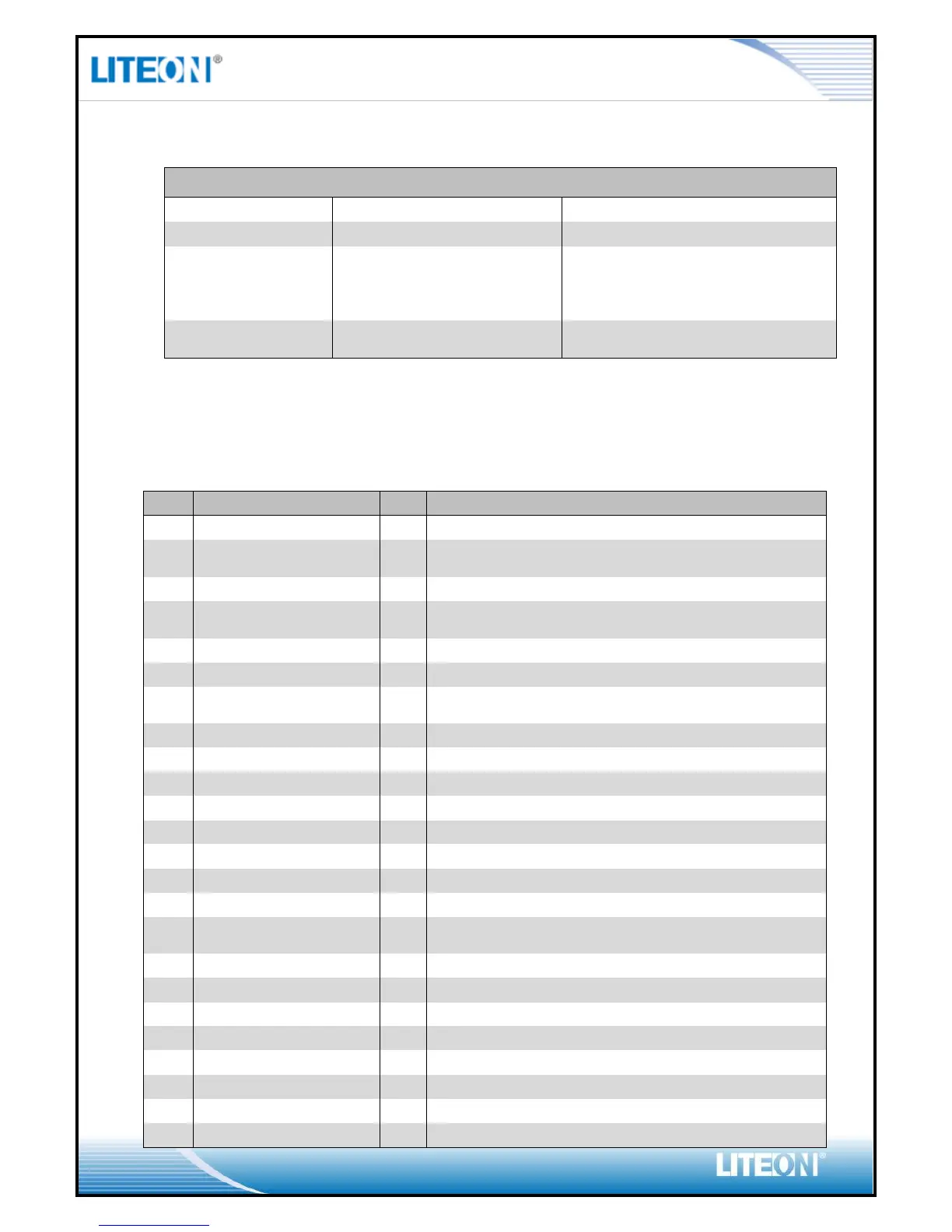
RECOMMENDED OPERATION CONDITIONS
Symbol
Parameter
Min
Typ
Max
Units
VDD33
3.3V Supply Voltage
3.14
3.3
3.46
V
VDD33_SWREG_VIN
Supply Voltage for internal PMU
3.14
3.3
3.46
V
VDDIO_GPIO0
VDDIO_GPIO1
VDDIO_GPIO2
VDDIO_AO_IN
Voltage supply for all IO signals
1.71
3.14
1.8
3.3
1.89
3.46
V
AVDD11
1.1V supply from internal 1.1V
PMU
1.05
1.1
1.2
V
PIN ASSIGMENT
* The following signal type is defined:
I: Input; O: Output; I/O: Input/Output; G: Ground
Pin.
Pin Define
I/O
Description
Status
1
GND
G
Ground
YES
2
AVDD11
I
Analog 1.1V input from Pin#28 of Module
(Host no need to connect)
NC
3
GND
G
Ground
YES
4
VDD33_WL_PA1
I
3.3V Power for both 2.4GHz/5GHz PA in
WLAN Chain 1
YES
5
VDD33
I
3.3V power for WLAN
YES
6
GND
G
Ground
YES
7
VDDIO_XTAL
I
Share same voltage of VDDIO_AO_IN
(Pin#32)
YES
8
BT_UART_CTS
I
UART Clear to Send for BT interface
YES
9
BT_UART_TXD
O
UART Transmit Data for BT interface
YES
10
HOST_WAKEUP_BT#
I
Host wake up BT of QCA9379-3, Low Active
YES
11
BT_UART_RXD
I
UART Receive Data for BT interface
YES
12
BT_PCM_SYN
I
PCM synchronous for BT
YES
13
BT_PCM_OUT
O
PCM Data out for BT
YES
14
BT_UART_RTS
O
UART Ready to Send for BT interface
YES
15
BT_PCM_CLK
I
PCM Clock for BT
YES
16
AVDD11
I
Analog 1.1V input from Pin#28 of Module
(Host no need to connect)
NC
17
BT_PCM_IN
I
PCM Data in for BT. 10K PU in the module
YES
18
VDDIO_GPIO1
I
1.8V or 3.3V upon signal interface
YES
19
RESERVED
NC
20
RESERVED
NC
21
VDDIO_GPIO0
I
Can be 1.8V (SDIO3.0) or 3.3V (SDIO2.0)
YES
22
SDOI_DATA3
I/O
SDIO Data Line3 for WLAN
YES
23
WOW#
O
WLAN wake up Host, Low Active
YES
24
SDIO_CLK
I
SDIO Clock for WLAN
YES

Related product manuals