4
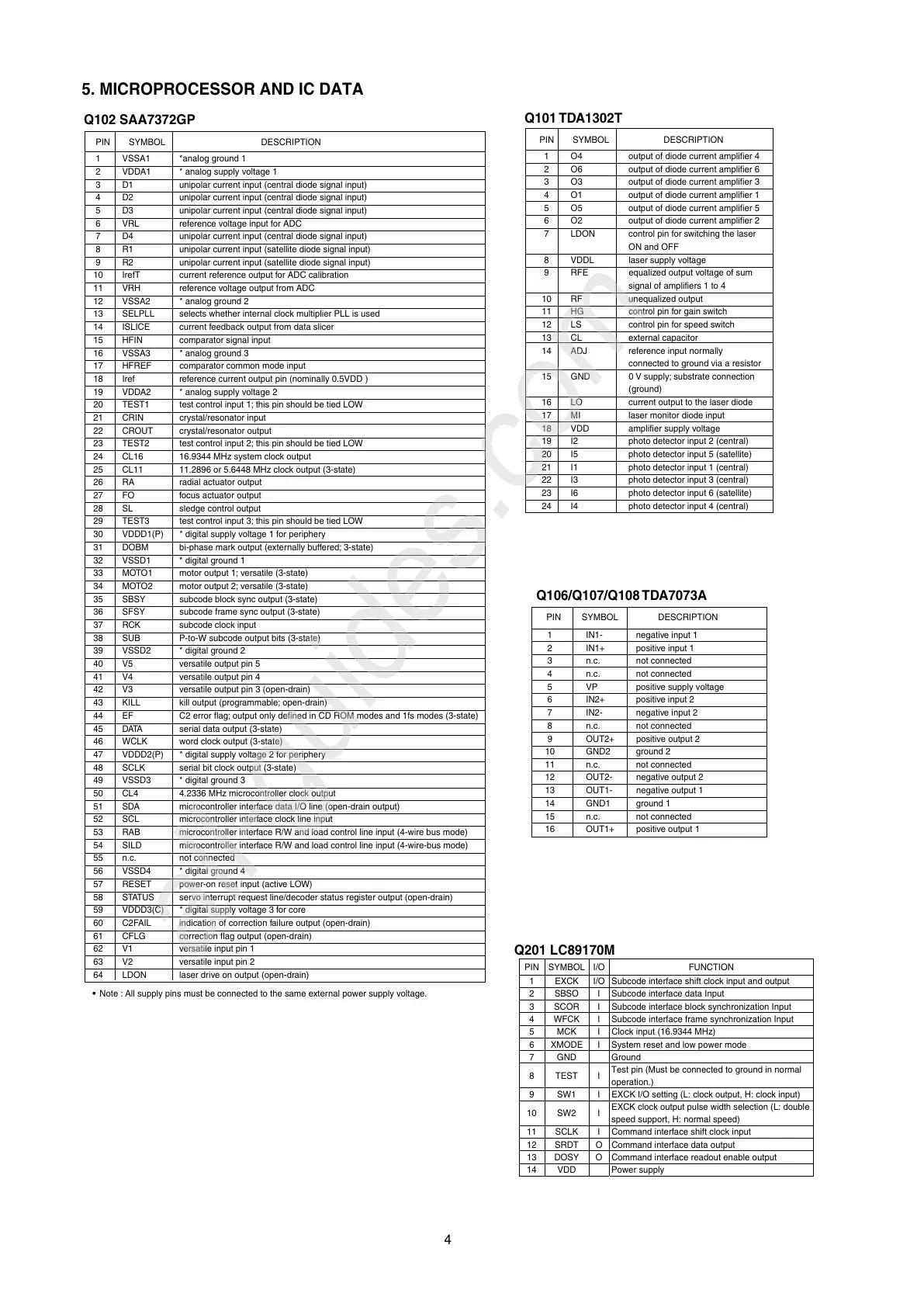
Q201 LC89170M
PIN SYMBOL I/O FUNCTION
1 EXCK I/O Subcode interface shift clock input and output
2 SBSO I Subcode interface data Input
3 SCOR I Subcode interface block synchronization Input
4 WFCK I Subcode interface frame synchronization Input
5 MCK I Clock input (16.9344 MHz)
6 XMODE I System reset and low power mode
7 GND Ground
8 TEST I
Test pin (Must be connected to ground in normal
operation.)
9 SW1 I EXCK I/O setting (L: clock output, H: clock input)
10 SW2 I
EXCK clock output pulse width selection (L: double
speed support, H: normal speed)
11 SCLK I Command interface shift clock input
12 SRDT O Command interface data output
13 DOSY O Command interface readout enable output
14 VDD Power supply
1 IN1- negative input 1
2 IN1+ positive input 1
3 n.c. not connected
4 n.c. not connected
5 VP positive supply voltage
6 IN2+ positive input 2
7 IN2- negative input 2
8 n.c. not connected
9 OUT2+ positive output 2
10 GND2 ground 2
11 n.c. not connected
12 OUT2- negative output 2
13 OUT1- negative output 1
14 GND1 ground 1
15 n.c. not connected
16 OUT1+ positive output 1
PIN SYMBOL DESCRIPTION
Q106/Q107/Q108 TDA7073A
1 O4 output of diode current amplifier 4
2 O6 output of diode current amplifier 6
3 O3 output of diode current amplifier 3
4 O1 output of diode current amplifier 1
5 O5 output of diode current amplifier 5
6 O2 output of diode current amplifier 2
7 LDON control pin for switching the laser
ON and OFF
8 VDDL laser supply voltage
9 RFE equalized output voltage of sum
signal of amplifiers 1 to 4
10 RF unequalized output
11 HG control pin for gain switch
12 LS control pin for speed switch
13 CL external capacitor
14 ADJ reference input normally
connected to ground via a resistor
15 GND 0 V supply; substrate connection
(ground)
16 LO current output to the laser diode
17 MI laser monitor diode input
18 VDD amplifier supply voltage
19 I2 photo detector input 2 (central)
20 I5 photo detector input 5 (satellite)
21 I1 photo detector input 1 (central)
22 I3 photo detector input 3 (central)
23 I6 photo detector input 6 (satellite)
24 I4 photo detector input 4 (central)
PIN SYMBOL DESCRIPTION
Q101 TDA1302T
1 VSSA1 *analog ground 1
2 VDDA1 * analog supply voltage 1
3 D1 unipolar current input (central diode signal input)
4 D2 unipolar current input (central diode signal input)
5 D3 unipolar current input (central diode signal input)
6 VRL reference voltage input for ADC
7 D4 unipolar current input (central diode signal input)
8 R1 unipolar current input (satellite diode signal input)
9 R2 unipolar current input (satellite diode signal input)
10 IrefT current reference output for ADC calibration
11 VRH reference voltage output from ADC
12 VSSA2 * analog ground 2
13 SELPLL selects whether internal clock multiplier PLL is used
14 ISLICE current feedback output from data slicer
15 HFIN comparator signal input
16 VSSA3 * analog ground 3
17 HFREF comparator common mode input
18 Iref reference current output pin (nominally 0.5VDD )
19 VDDA2 * analog supply voltage 2
20 TEST1 test control input 1; this pin should be tied LOW
21 CRIN crystal/resonator input
22 CROUT crystal/resonator output
23 TEST2 test control input 2; this pin should be tied LOW
24 CL16 16.9344 MHz system clock output
25 CL11 11.2896 or 5.6448 MHz clock output (3-state)
26 RA radial actuator output
27 FO focus actuator output
28 SL sledge control output
29 TEST3 test control input 3; this pin should be tied LOW
30 VDDD1(P) * digital supply voltage 1 for periphery
31 DOBM bi-phase mark output (externally buffered; 3-state)
32 VSSD1 * digital ground 1
33 MOTO1 motor output 1; versatile (3-state)
34 MOTO2 motor output 2; versatile (3-state)
35 SBSY subcode block sync output (3-state)
36 SFSY subcode frame sync output (3-state)
37 RCK subcode clock input
38 SUB P-to-W subcode output bits (3-state)
39 VSSD2 * digital ground 2
40 V5 versatile output pin 5
41 V4 versatile output pin 4
42 V3 versatile output pin 3 (open-drain)
43 KILL kill output (programmable; open-drain)
44 EF C2 error flag; output only defined in CD ROM modes and 1fs modes (3-state)
45 DATA serial data output (3-state)
46 WCLK word clock output (3-state)
47 VDDD2(P) * digital supply voltage 2 for periphery
48 SCLK serial bit clock output (3-state)
49 VSSD3 * digital ground 3
50 CL4 4.2336 MHz microcontroller clock output
51 SDA microcontroller interface data I/O line (open-drain output)
52 SCL microcontroller interface clock line input
53 RAB microcontroller interface R/W and load control line input (4-wire bus mode)
54 SILD microcontroller interface R/W and load control line input (4-wire-bus mode)
55 n.c. not connected
56 VSSD4 * digital ground 4
57 RESET power-on reset input (active LOW)
58 STATUS servo interrupt request line/decoder status register output (open-drain)
59 VDDD3(C) * digital supply voltage 3 for core
60 C2FAIL indication of correction failure output (open-drain)
61 CFLG correction flag output (open-drain)
62 V1 versatile input pin 1
63 V2 versatile input pin 2
64 LDON laser drive on output (open-drain)
PIN SYMBOL DESCRIPTION
Note : All supply pins must be connected to the same external power supply voltage.
Q102 SAA7372GP
5. MICROPROCESSOR AND IC DATA
 Loading...