47
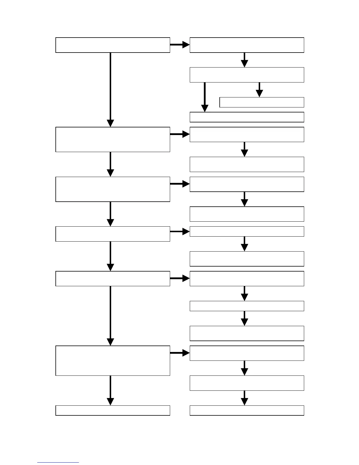
3.5 Check the Video encoder. (Component, CVBS, Y/C)
OK
OK
OK
OK
NG
OK
NG
NG
OK
NG
OK
OK
OK
OK
Finish
NG
OK
OK
NG
OK
NG
OK
OK
Are the VD+3.3V and +2.5AD voltage lines
of QM01 normal?
Is the reset signal of QM01 (33pin)
normal?
VRST_5=H
Are the digital data of QM01 normal?
2-9pin, 12-18pin, 26-30pin, 51-55pin and
58-62pin
Is the master clock waveform of 32pin on
QM01 normal? 27MHz 2Vp-p
Is the IIC waveform of 21pin and 22pin on
QM01 normal?
Are the video signals outputted to each pin
of JM01?
1pin=video, 3pin=S-C, 5pin=S-Y,
7pin=component-Y, 9pin=Cb, 11pin=Cr
Check the soldering of QM01, LM01, LM02,
LM03, QK91 and QM91.
Check the input voltage of QK91 and QM91.
Replace QK91 or QM92.
Refer to “POWER SUPPLY PCB”.
Check the soldering of QK10 (18pin),
RM12 and CM09.
Refer to “3.4 Check the DIGITAL VIDEO
OUTPUT”.
Check the soldering of RM01-05, RM26-29
and QM01.
Refer to “3.4 Check the DIGITAL VIDEO
OUTPUT”.
Check the soldering of RM11 and QM01.
Refer to “3.4 Check the DIGITAL VIDEO
OUTPUT”.
Check the soldering of RM08, RM09 and
QM01.
Check the soldering of QK07 and QK08.
Refer to “3.4 Check the DIGITAL VIDEO
OUTPUT”.
Check the soldering of QM02-QM07 and
circumference resistors.
Check the output signals of QM01
(37-39 pin and 42-44pin).
Replace QM02-QM07.