89
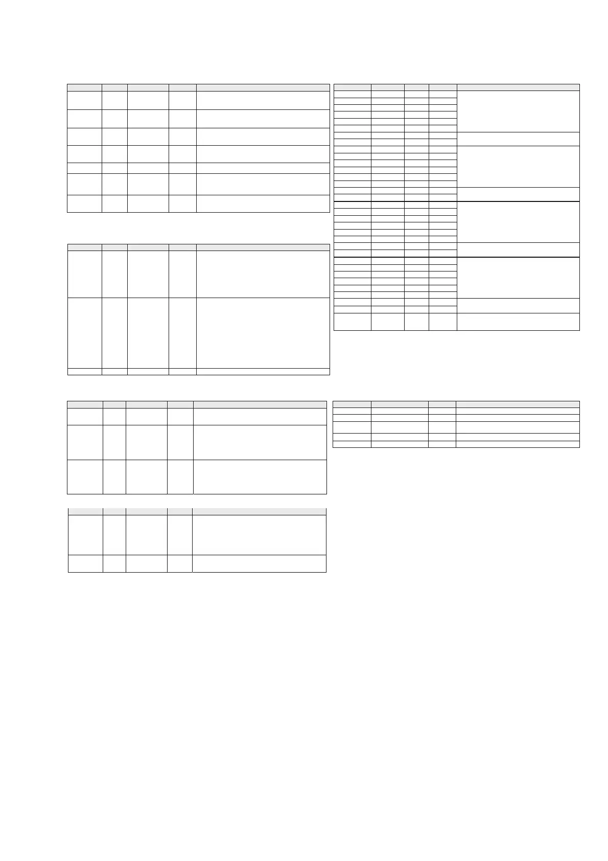
System Switching Pins
Pin Name Pin # Type Dir Description
DSDA0,
DSDA1,
DSDA2
30,
50,
70
LVTTL,
Schmitt Trigger,
5V tolerant
Input/
Output
DDC I
2
C Data for respective port. Note 1.
DSCL0,
DSCL1,
DSCL2
31,
51,
71
LVTTL,
Schmitt Trigger,
5V tolerant
Input DDC I
2
C Clock for respective port. Note 1.
RPWR0,
RPWR1,
RPWR2
32,
52,
72
LVTTL,
5V Tolerant
Input 5V Port detection input for respective port.
Connect to 5V signal from HDMI input connector.
HPD0,
HDP1,
HPD2
16,
36,
56
LVTTL, 2mA,
5V Tolerant
Output Hot Plug Detect Output for respective port.
Connect to HOTPLUG of HDMI input connector.
HPDIN 76
LVTTL,
5V Tolerant
Input Hot Plug Detect Input.
TSCL 78
LVTTL,
Schmitt Trigger.
Open Drain
5V tolerant
Output Master DDC I
2
C Clock (Open Drain Output) to HDMI receiver.
I
2
C transactions required for HDCP operation are performed
over this I
2
C bus. Note 1.
TSDA 77
LVTTL,
Schmitt Trigger,
5V tolerant
Input/
Output
Master DDC Data (Open drain output.) to HDMI receiver. I
2
C
transactions required for HDCP operation are performed over
this I
2
C bus. Note 1.
Note:
1. These signals are true open drain, and do not pull to ground when power is not applied to the device. These signals
require an external pull-up.
Configuration Pins
Pin Name Pin # Type Dir Description
I2CADDR/
TPWR
79 LVTTL, 4mA,
5V Tolerant
Input/
Output
I
2
C Slave Address input / Transmit Power Sense output pin.
When RESET# is low, this pin is used as an input to latch the
I
2
C sub-address. The level on this pin is latched when the
RESET# pin transitions from low to high.
When RESET# is high, this pin is used as the TPWR output,
indicating that the selected Rx-port is has 5V present. When
none of the Rx ports are selected, this signal is low.
See page 15 for more information.
I2CSEL/INT# 35 Schmitt Trigger,
Open Drain, 4mA,
5V Tolerant
Input/
Output
I
2
C Selection input / Interrupt output pin.
When RESET# is low, this pin is used as an input to latch the
External Port Detection signal. The level on this pin is latched
when the RESET# pin transitions from low to high.
When this pin is high during reset, the external pins
EPSEL1/LSCL and EPSEL0/LSDA are used to select the Rx-
port as EPSEL[1:0].
When this pin is low during reset, the internal local I
2
C register
is used to select the Rx-port.
After reset, this pin becomes the Interrupt output.
This is an open-drain output and requires an external pull-up.
See page 14 for more information.
RSVDL 75 Input Reserved for use by Silicon Image and must be tied low.
Control Pins
Pin Name Pin # Type Dir Description
RESET# 13 LVTTL,
Schmitt Trigger.
5V tolerant
Input Reset Pin (Active LOW). Certain configuration inputs are
latched when RESET# transitions from low to high. See page
14 for more information.
LSCL/EPSEL1 15 Schmitt
5V tolerant
Input Local I
2
C Clock / External Port Select 1. When I2CSEL is high,
this becomes the Local I
2
C bus clock pin, LSCL. When I2CSEL
is low, this becomes the external port select pin, EPSEL1. True
open drain, so does not pull to ground if power not applied. An
external pull-up is required.
See page 14 for more information.
LSDA/EPSEL0 14 LVTTL,
Schmitt Trigger.
Open Drain
5V tolerant
Input/
Output
Local I
2
C Data / External Port Select 0. When I2CSEL is high,
this becomes the Local I
2
C bus data pin, LSDA. When I2CSEL
is low, this becomes the external port select pin, EPSEL0. True
open drain, so does not pull to ground if power not applied. An
external pull-up is required.
See page 14 for more information.
CEC Pins
Pin Name Pin # Type Direction Description
CEC_A 54 CEC Compliant,
5V tolerant.
Input/
Output
HDMI compliant CEC I/O used to interface to CEC devices.
CEC electrically compliant signal. This pin connects to the CEC
signal of all HDMI connectors in the system.
As an input, the pad acts as a LVTTL Schmitt triggered input
and is 5V tolerant. As an output, the pad acts as an NMOS
driver with resistive pull-up. This pin has an internal pull-up
resistor.
CEC_D 53 LVTTL,
Schmitt Trigger
5V tolerant.
Input/
Output
CEC interface to local system. True open-drain. An external
pull-up is required. This pin typi
cally connects to the local CPU.
Differential Signal Data Pins
Pin Name Pin # Type Dir Description
R0X0+ 22 TMDS Input
R0X0- 21 TMDS Input
R0X1+ 25 TMDS Input
R0X1- 24 TMDS Input
R0X2+ 28 TMDS Input
R0X2- 27 TMDS Input
TMDS input Port 0 data pairs.
R0C+ 19 TMDS Input
R0C- 18 TMDS Input
TMDS input Port 0 clock pair.
R1X0+ 42 TMDS Input
R1X0- 41 TMDS Input
R1X1+ 45 TMDS Input
R1X1- 44 TMDS Input
R1X2+ 48 TMDS Input
R1X2- 47 TMDS Input
TMDS input port 1 data pairs.
R1C+ 39 TMDS Input
R1C- 38 TMDS Input
TMDS input Port 1 clock pair.
R2X0+ 62 TMDS Input
R2X0- 61 TMDS Input
R2X1+ 65 TMDS Input
R2X1- 64 TMDS Input
R2X2+ 68 TMDS Input
R2X2- 67 TMDS Input
TMDS input port 2 data pairs.
R2C+ 59 TMDS Input
R2C- 58 TMDS Input
TMDS input Port 2 clock pair.
TX0+ 7 TMDS Output
TX0- 8 TMDS Output
TX1+ 4 TMDS Output
TX1- 5 TMDS Output
TX2+ 1 TMDS Output
TX2- 2 TMDS Output
TMDS output data pairs.
TXC+ 10 TMDS Output
TXC- 11 TMDS Output
TMDS output clock pair.
EXT_SWING 12 Analog Input Voltage Swing Adjust. A resistor tied from this pin to
AVCC18 determines the amplitude of the voltage swing.
The recommended value is 500ȍ
.
Power and Ground Pins
Pin Name Pin # Type Description
AVCC33 23, 43, 55, 63 Power Analog VCC. Connect to 3.3V supply.
AVCC18 6, 17, 29, 37, 49, 57, 69 Power
Analog VCC. Connect to 1.8V supply.
AGND 3, 9, 20, 26, 40,
46, 60, 66, 80
Ground Analog GND.
DVCC18 33, 73 Power Digital VCC. Connect to 1.8V supply.
DGND 34, 74 Ground Digital GND.
IC81 : Sil 9185
 Loading...