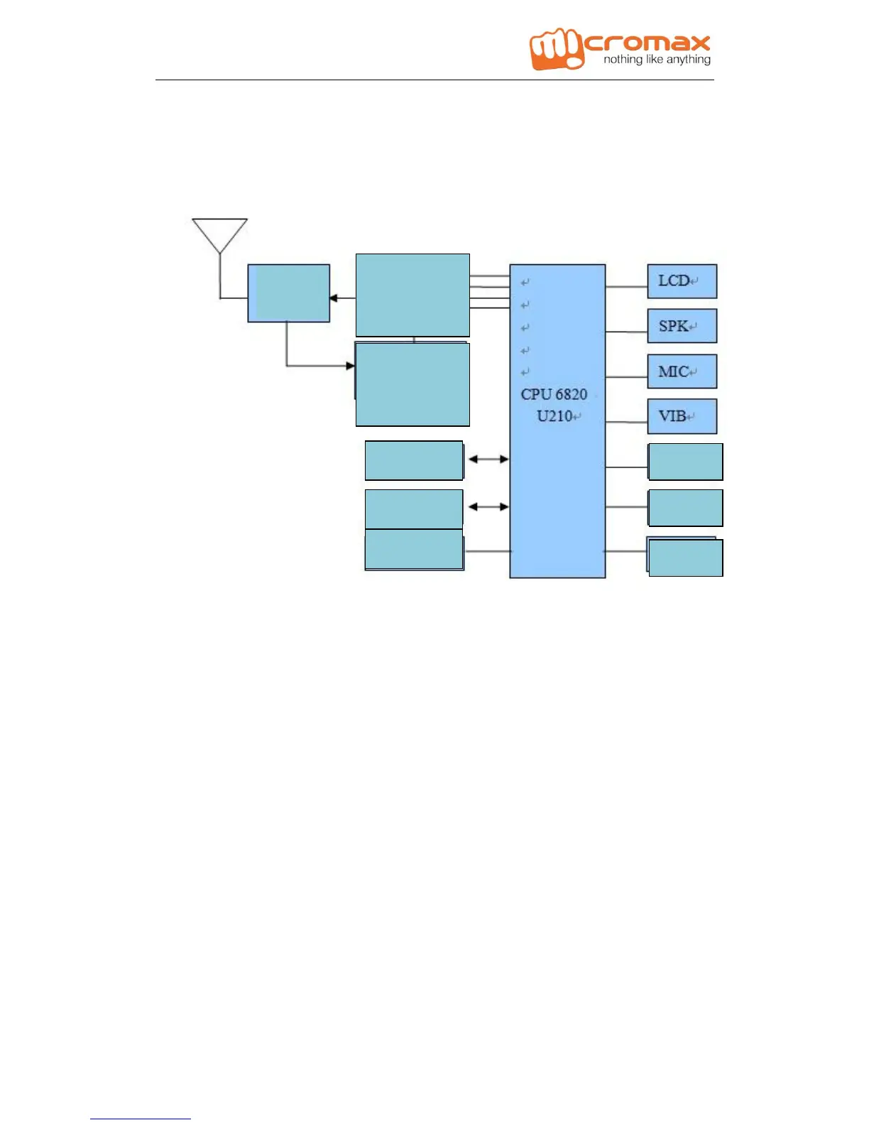
1.2 Detailed Description of Circuit Chart
1.3 RF circuit
This phone is designed on SC6820 platform. RF main chip integration SR1019,
PA use RDA6163A, TCXO uses 26MHz crystal oscillator.
(1) Receiving circuit
The GSM or DCS signal received from a base station via antenna is inputted from
the pin 27 of U101, send U104/U105 to pin A20/B20/A19/B19. This chip integrates
LNA and Frequency mixer. The signals are amplified by their own low-noise
amplifier (LNA). The amplified signal is sent to a down converter, where the signal is
mixed with local oscillation (LO) output from RX VCO to generate zero intermediate
frequency (ZIF) signals. The zero-IF signal passes through a filter and is amplified by
programmable gain amplifier (PGA), then the signal is outputted to I and Q
demodulator to generate I/Q base band signals.
(2) Transmitting circuit
A transmitter consists of I/Q modulation circuit, up-conversion mixer circuit,