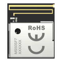
MS50SF7
Specification V1.0
www.minewsemi.com minewsemi@minew.com Copyright
©
Shenzhen Minewsemi Co., Ltd.
This manual and all the contents contained in it are owned by Shenzhen Minewsemi Co., Ltd. and are protected by Chinese laws and applicable international conventions related to
copyright laws.The company has the right to change the content of this manual according to the technological development, and the revised version will not be notified otherwise.
Without the written permission and authorization of the company, any individual, company, or organization shall not modify the contents of this manual or use part or all of the
contents of this manual in other ways. Violators will be held accountable in accordance with the law.
Layout notes
:
1) Preferred Module antenna area completely clearance and not be prevented by metals,
otherwise it will influence antenna’s effect (as above DWG. indication).
2) Cover the external part of module antenna area with copper as far as possible to reduce
the main board’s signal cable and other disturbing.
3) It is preferred to have a clearance area of 4 square meter or more area around the module
antenna (including the shell) to reduce the influence to antenna.
4) Device should be grounded well to reduce the parasitic inductance.
5) Do not cover copper under module’s antenna in order to avoid affect signal radiation or
lead to transmission distance affected.
6) Antenna should keep far from other circuits to prevent radiation efficiency reduction or
affects the normal operation of other lines.
7) Module should be placed on edge of circuit board and keep a distance away from other
circuits.
8) Suggesting to use magnetic beads to insulate module’s access power supply.
 Loading...