59
7521
7521
N/B MAINTENANCE
N/B MAINTENANCE
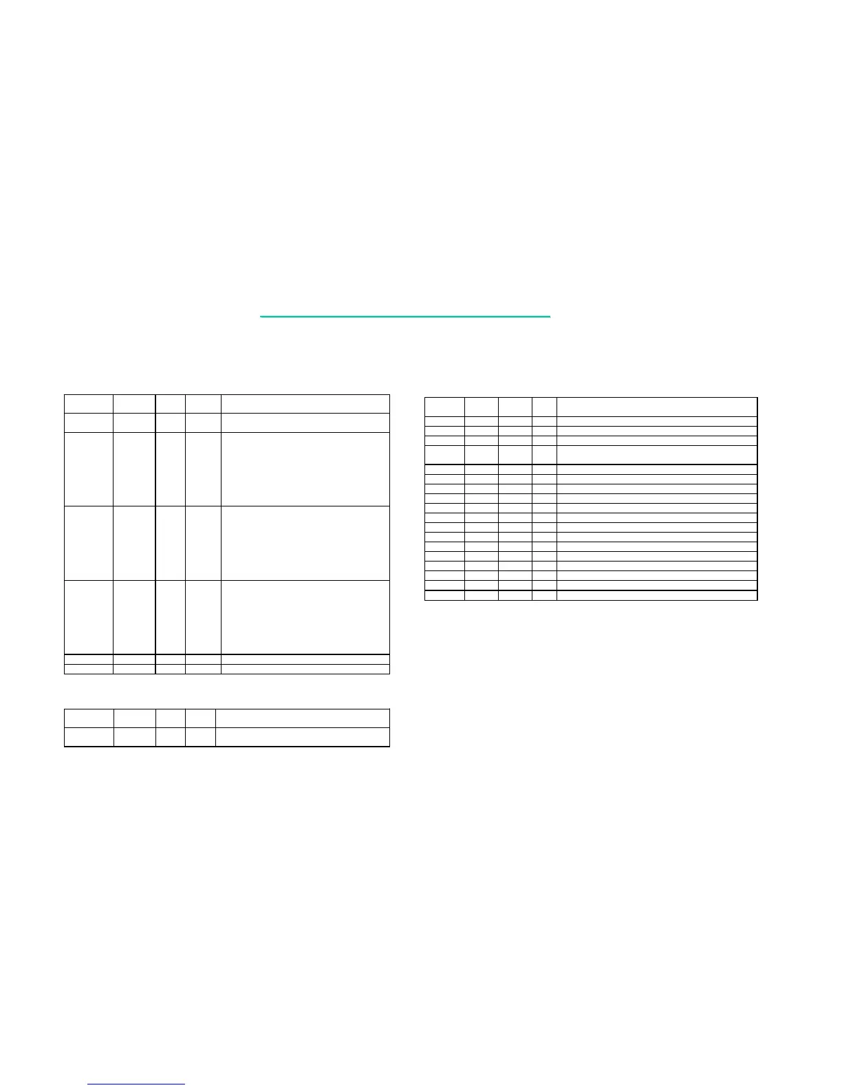
USB interface
Name Tolerance Power
Plane
Type
Attr
Description
CLK48M 3.3V/5V MAIN I USB 48 MHz clock input : This signal provides
the fundamental clock for the USB Controller.
OC0#
PCIREQ3#
GPIO0
3.3V/5V MAIN I
I
I/O/OD
USB Port 0 Over Current Detection : OC0# is
used to detect the over current condition of USB
Port 0.
External PCI Master Request 3: PCIREQ3# is
used for PCI Device on PCI Slot 3 to assert its
request to hold PCI Bus.
General Purpose Input/Output 0 : Refer to GPIO
description.
OC1#
PCIGNT3#
GPIO1
3.3V/5V MAIN I
O
I/O/OD
USB Port 1 Over Current Detection : OC1# is
used to detect the over current condition of USB
Port 1.
External PCI Master Grant 3 : PCIGNT3# is
used to indicate PCI Device on PCI Slot 3 the PCI
Bus has been granted.
General Purpose Input/Output 1 : Refer to GPIO
description.
OC3#
LDRQ1#
GPIO2
3.3V/5V MAIN I
I
I/O/OD
USB Port 3 Over Current Detection: OC3# is
used to detect the over current condition of USB
Port 3.
LPC DMA Request 1 : LDRQ1# is the second
LPC DMA request signal used by LPC Device to
request DMA cycles.
General Purpose Input/Output 2 : Refer to GPIO
description.
USBP[4:0]P 3.3V AUX I/O USB Port [4:0] Positive Input/Output
USBP[4:0]N 3.3V AUX I/O USB Port [4:0] Negative Input/Output
Legacy I/o and Miscellaneous Signals
Name Tolerance Power
Plane
Type
Attr
Description
SPK 3.3V MAIN O Speaker output : The SPK is connected to the
system speaker.
Power and Ground Signals
Name Tolerance Power
Plane
Typ e
Attr
Des cri pt i on
VSS
GROUND 0V
IVDD
MAIN 1 . 8V
IVDD (AUX)
AUX 1 . 8 V
OVDD
(AUX)
AUX 3 . 3 V
USBVDD
AUX 3 . 3 V
RTCVDD
RT C 1 .8 V
DCLKAVDD
MAIN 3 . 3V
ECLKAVDD
MAIN 3 . 3V
TXAVDD
AUX 3 . 3 V
RXAVDD
AUX 3 . 3 V
DACAVDD
MAIN 3 . 3V
IDEAVDD
MAIN 1 . 8V
SDAVDD
MAIN 3 . 3V
CPUAVDD
MAIN 3 . 3V
VTTB
MAIN 1 . 5V
VSSQ
GROUND 0V
VTTA
MAIN 1 . 5V
VCC3
MAIN 3 . 3V
4. Pin Descriptions Of Major Components
4.2 SiS630 Slot 1/Socket 370 2D/3D Ultra-AGP™ Single Chipset
 Loading...