APPENDICES
Appendix 2 Special Register List
App - 60
9
Parameters
10
Device Explanation
11
CPU Module Processing
Time
12
Procedure for Writing
Program to CPU ModuleAppendicesIndex
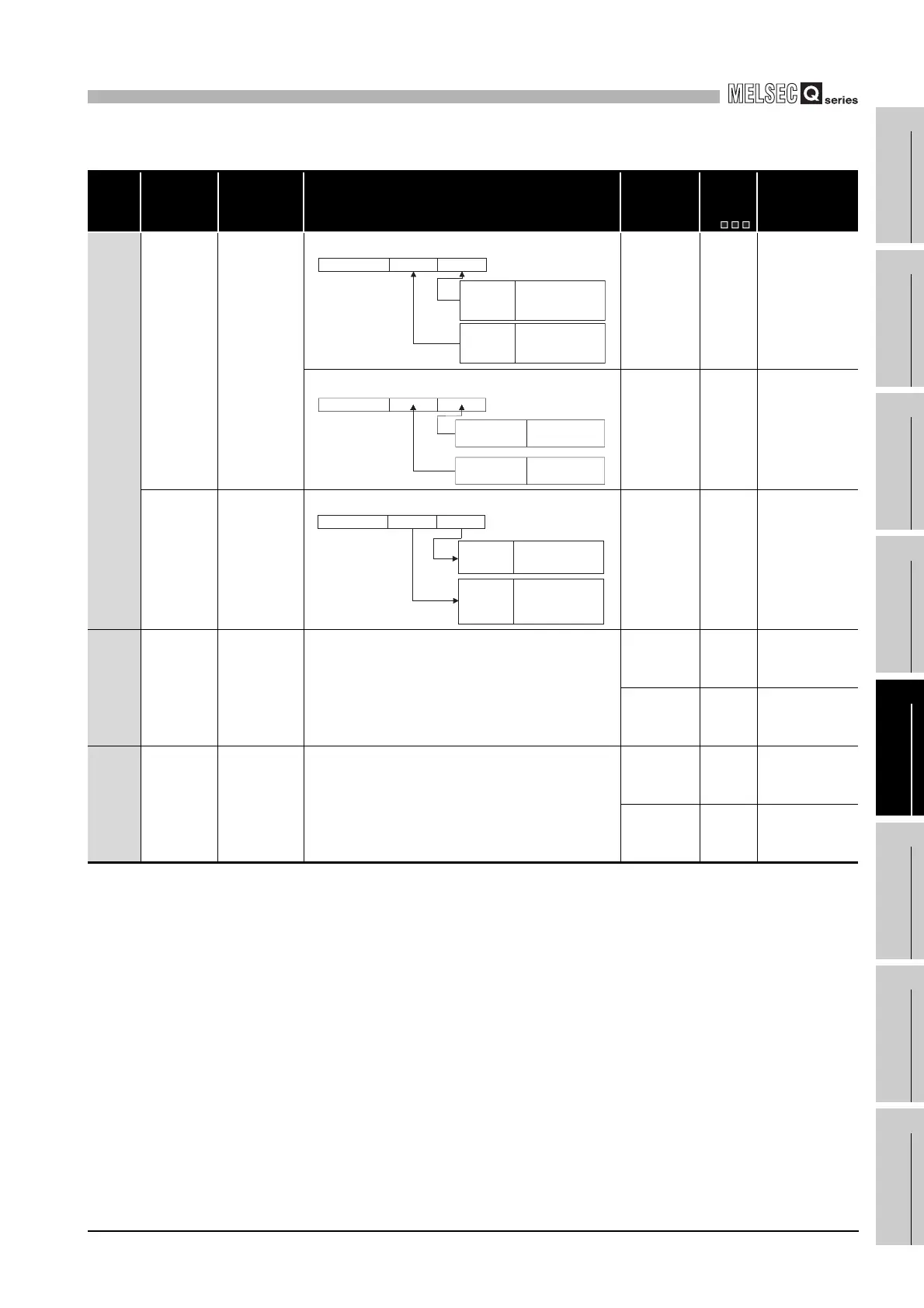
TableApp.24 Special register
Number Name Meaning Explanation
Set by
(When Set)
Corres-
ponding
ACPU
D9
Corresponding
CPU
SD620
Drive 3/4 typs Drive 3/4 typs
• Indicates the drive 3/4 type.
S (Initial) New
Qn(H)
QnPH
QnPRH
QnU
• Indicates the drive 3/4 type.
S (Initial) New Q00J/Q00/Q01
Memory card B
typs
Memory card B
typs
• Indicates memory card B type installed
S (Initial/Card
installation and
removal)
New
Q2A(S1)
Q3A
Q4A
Q4AR
SD622
Drive 3
(Standard RAM)
capacity
Drive 3 capacity
• Drive 3 capacity is stored in 1 k byte units.
(Empty capacity after format is stored.)
S (Initial) New
Qn(H)
QnPH
QnPRH
QnU
S (Initial/Card
installation and
removal)
New
Q2A(S1)
Q3A
Q4A
Q4AR
SD623
Drive 4
(Standard
ROM) capacity
Drive 4 capacity
• Drive 4 capacity is stored in 1 k byte units.
(Empty capacity after format is stored.)
S (Initial) New
Qn(H)
QnPH
QnPRH
QnU
S (Initial/Card
installation and
removal)
New
Q2A(S1)
Q3A
Q4A
Q4AR
0
b7
b4 b0
b15 b8
to to
Drive 3
(Standrd
RAM)
Fixed to 1
Drive 4
(Standrd
ROM)
Fixed to 3
b3
to
b4 b3 b0
0
b8 b7b15
to toto
Drive 3
(Standard RAM)
Drive 4
(Standrd ROM)
0: Absent
1: Present
Fixed to
"3 (FLASH ROM)"
0
b7
b4 b0
b15 b8
to to
Drive 3
(RAM)
Drive 4
(ROM)
b3
to
0: Does not exist
1: SRAM
0: Does not exist
2: E
2
PROM
3: Flash ROM
 Loading...