Do you have a question about the Motorola CM200 and is the answer not in the manual?
Information on radio safety and compliance with RF energy exposure limits.
Details the manual's purpose, intended audience, and currency.
Outlines Motorola's product support, including warranty and out-of-warranty services.
Provides information on how to order replacement parts and equipment.
Explains how to determine radio model characteristics from the model number.
Introduces the chapter's content on maintenance procedures and safety.
Recommends periodic visual inspection and cleaning for radio maintenance.
Details checks for external surfaces and controls to ensure functionality.
Describes recommended cleaning agents and methods for external and internal surfaces.
Provides precautions for handling sensitive CMOS and LDMOS devices to prevent damage.
Covers procedures for parts replacement, substitution, and soldering techniques.
Lists recommended service aids and test equipment for radio servicing.
Details essential test equipment required for servicing radios.
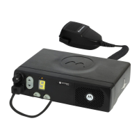
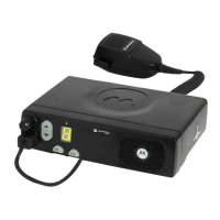
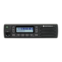
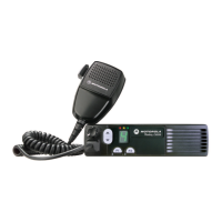
Describes the CM200 control head features and indicators.
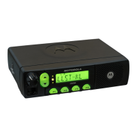
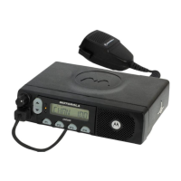
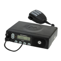
Describes CM300/PM400 control heads with LCD displays and indicators.
Introduces the theory of operation for control head circuits and troubleshooting.
Details the CM200 control head components and their functions.
Explains the power supply distribution within the CM200 control head.
Describes the Serial Peripheral Interface communication between radio and head.
Explains the four-key keypad design and analog line reading by the µP.
Details how indicator LEDs and keypad backlighting are controlled.
Describes the MIC_PTT, dual-function lines, and HOOK line signals.
Explains the control head speaker function and its connection.
Describes electrostatic transient protection for sensitive components using diodes.
Details the CM300/PM400 control head components and their functions.
Explains the power supply distribution within the CM300/PM400 control head.
Describes the Serial Peripheral Interface communication for CM300/PM400.
Explains the keypad design and analog line reading for CM300/PM400.
Describes the LCD control via U3 and SPI bus communication.
Details LED status control and LCD/key backlighting for CM300/PM400.
Describes MIC_PTT, dual-function lines, and HOOK line signals for CM300/PM400.
Explains the control head speaker function for CM300/PM400.
Describes electrostatic transient protection for sensitive components in CM300/PM400.
Provides a flowchart for troubleshooting CM200 control head failures.
Details steps to diagnose general control head failures in CM200.
Outlines troubleshooting for button/tones select errors in CM200 (Part 1).
Continues troubleshooting for button/tones select errors in CM200 (Part 2).
Provides a flowchart for troubleshooting CM300/PM400 control head failures.
Details steps to diagnose general control head failures in CM300/PM400.
Outlines troubleshooting for button/tones select errors in CM300/PM400 (Part 1).
Continues troubleshooting for button/tones select errors in CM300/PM400 (Part 2).
Indexes schematics, layouts, and parts lists for control heads.
Presents PCB layout and schematic diagrams for the CM200 control head.
Lists all parts for the CM200 control head PCB 8488998U01.
Presents PCB layout and schematic diagrams for CM300/PM400 control heads.
Provides a chart detailing models, items, and descriptions for radios.
Lists general, transmitter, and receiver specifications for UHF2 radios.
Introduces the theory of operation for UHF2 circuits and controller circuits.
Explains the theory of operation for the UHF2 receiver front-end and back-end.
Details the signal path from antenna input to the first mixer.
Describes UHF2 IF signal amplification, filtering, and demodulation.
Explains the three-stage LDMOS transmitter power amplifier for UHF2.
Describes the 24 dB gain integrated circuit amplifier and its control.
Details the LDMOS driver stage gain and bias control.
Explains the LDMOS final stage bias and matching network.
Describes the microstrip printed circuit that couples RF power.
Explains the operation of the antenna switch utilizing PIN diodes.
Describes the low-pass filter for attenuating harmonic energy.
Explains UHF2 output power regulation using a forward power detection loop.
Details the synthesizer components: reference oscillator, LVFRAC-N, and VCO.
Describes the crystal-controlled oscillator and its frequency compensation.
Explains the LVFRAC-N synthesizer components and function.
Details the VCO/Buffer IC, tank circuits, and modulation.
Explains the synthesizer operation, including phase detector and loop filter.
Explains the radio's components and control head connection.
Details the five separate devices providing voltage distribution.
Explains protection against ESD, voltage polarity, and load dump.
Describes the three ways the radio can be switched ON.
Explains clock source generation by ASFIC CMP and µP reprogramming.
Describes the µP communication to ICs via the SPI port.
Explains the SBEP interface for radio communication with CPS or tuner.
Details the six general purpose I/O lines for external options.
Explains microprocessor operation modes and memory access.
Describes SRAM's role in temporary radio calculations.
Covers audio signalling filter IC and compander functions.
Details the four functions of the ASFIC CMP used in the controller.
Explains transmit audio paths and processing.
Describes the two distinct microphone input paths and their biasing.
Explains PTT sensing and audio processing for transmit.
Covers three types of hardware signaling: sub-audible, DTMF, and audible.
Explains sub-audible data signaling below 300 Hz.
Describes high speed data waveforms used in trunking systems.
Explains DTMF data used for phone interconnect operation.
Explains the receive audio paths and processing.
Details the squelch detection circuitry and logic outputs.
Describes receiver audio path processing and digital volume control.
Explains the audio power amplifier function and speaker outputs.
Describes handset audio availability at the control head connector.
Explains filtered and unfiltered audio paths and gain determination.
Covers receive signaling circuits including PL/DPL and high-speed data decoders.
Explains filtering and limiting of received data for MDC and high-speed data.
Describes alert tone generation and routing for operator feedback.
A flowchart for troubleshooting receiver RF issues (Sheet 1).
A flowchart for troubleshooting receiver issues (Sheet 2).
Flowchart for troubleshooting 40W transmitter power issues (Sheet 1).
Flowchart for troubleshooting 40W transmitter power/current issues (Sheet 2).
Flowchart for troubleshooting 40W transmitter TXing issues (Sheet 3).
Flowchart for diagnosing synthesizer operational problems.
Flowchart for diagnosing voltage controlled oscillator issues.
Flowchart for troubleshooting DC supply voltages (Part 1).
Flowchart for troubleshooting DC supply voltages (Part 2).
Indexes schematics, layouts, and parts lists for UHF2 and controller circuits.
Identifies schematics for UHF2 circuits and controller components.
Provides PCB layout and schematic diagrams for UHF2 1-25W radios.
Details PM400 models, items, and descriptions for UHF3 radios.
Lists general, transmitter, and receiver specifications for UHF3 radios.
Introduces the theory of operation for UHF3 circuits and controller circuits.
Explains the theory of operation for the UHF3 receiver front-end and back-end.
Details the signal path from antenna input to the first mixer for UHF3.
Describes UHF3 IF signal amplification, filtering, and demodulation.
Explains the three-stage LDMOS transmitter power amplifier for UHF3.
Describes the 24 dB gain integrated circuit amplifier and its control for UHF3.
Details the LDMOS driver stage gain and bias control for UHF3.
Explains the LDMOS final stage bias and matching network for UHF3.
Describes the microstrip printed circuit that couples RF power for UHF3.
Explains the operation of the antenna switch utilizing PIN diodes for UHF3.
Describes the low-pass filter for attenuating harmonic energy for UHF3.
Explains UHF3 output power regulation using a forward power detection loop.
Details the synthesizer components for UHF3: oscillator, LVFRAC-N, and VCO.
Describes the crystal-controlled oscillator and its frequency compensation for UHF3.
Explains the LVFRAC-N synthesizer components and function for UHF3.
Details the VCO/Buffer IC, tank circuits, and modulation for UHF3.
Explains the synthesizer operation, including phase detector and loop filter.
Explains the radio's components and control head connection.
Details the five separate devices providing voltage distribution.
Explains protection against ESD, voltage polarity, and load dump.
Describes the three ways the radio can be switched ON.
Explains clock source generation by ASFIC CMP and µP reprogramming.
Describes the µP communication to ICs via the SPI port.
Explains the SBEP interface for radio communication with CPS or tuner.
Details the six general purpose I/O lines for external options.
Explains microprocessor operation modes and memory access.
Describes SRAM's role in temporary radio calculations.
Covers audio signalling filter IC and compander functions.
Details the four functions of the ASFIC CMP used in the controller.
Explains transmit audio paths and processing.
Describes the two distinct microphone input paths and their biasing.
Explains PTT sensing and audio processing for transmit.
Covers three types of hardware signaling: sub-audible, DTMF, and audible.
Explains sub-audible data signaling below 300 Hz.
Describes high speed data waveforms used in trunking systems.
Explains DTMF data used for phone interconnect operation.
Explains the receive audio paths and processing.
Details the squelch detection circuitry and logic outputs.
Describes receiver audio path processing and digital volume control.
Explains the audio power amplifier function and speaker outputs.
Describes handset audio availability at the control head connector.
Explains filtered and unfiltered audio paths and gain determination.
Covers receive signaling circuits including PL/DPL and high-speed data decoders.
Explains filtering and limiting of received data for MDC and high-speed data.
Describes alert tone generation and routing for operator feedback.
A flowchart for troubleshooting receiver RF issues (Sheet 1).
A flowchart for troubleshooting receiver issues (Sheet 2).
Flowchart for troubleshooting 40W transmitter power issues (Sheet 1).
Flowchart for troubleshooting 40W transmitter power/current issues (Sheet 2).
Flowchart for troubleshooting 40W transmitter TXing issues (Sheet 3).
Flowchart for diagnosing synthesizer operational problems.
Flowchart for diagnosing voltage controlled oscillator issues.
Flowchart for troubleshooting DC supply voltages (Part 1).
Flowchart for troubleshooting DC supply voltages (Part 2).
Indexes schematics, layouts, and parts lists for UHF2 and controller circuits.
Identifies schematics for UHF2 circuits and controller components.
Provides PCB layout and schematic diagrams for UHF2 1-25W radios.
Indexes schematics, layouts, and parts lists for UHF3 and controller circuits.
Identifies schematics for UHF3 circuits and controller components.
Provides PCB layout and schematic diagrams for UHF3 25-40W radios.
| Operating Temperature | -30°C to +60°C |
|---|---|
| Channel Spacing | 12.5/20/25 kHz |
| Waterproof | No |
| Frequency Range | VHF: 136-174 MHz / UHF: 403-470 MHz |
| Power Output | 1-25W (VHF) / 1-25W (UHF) |
| Battery Life | N/A (Mobile Radio) |