VHF (136-174MHz) Transmitter Power Amplifier (PA) 25 W 2-3
low IF signal is amplified and filtered by an external pair of 455 kHz ceramic filters FL3112, FL3114
for 20/25 kHz channel spacing or FL3111, FL3113/F3115 for 12.5 kHz channel spacing. These pairs
are selectable via BWSELECT. The filtered output from the ceramic filters is applied to the limiter
input pin of the IF IC (pin 14).
The IF IC contains a quadrature detector using a ceramic phase-shift element (Y3102) to provide
audio detection. Internal amplification provides an audio output level of 120 mV rms (at 60%
deviation) from U3101 pin 8 (DISCAUDIO) which is fed to the ASFIC_CMP (U0221) pin 2 (part of
the Controller circuitry).
A received signal strength indicator (RSSI) signal is available at U3101 pin 5, having a dynamic
range of 70 dB. The RSSI signal is interpreted by the microprocessor (U0101 pin 63) and in addition
is available at accessory connector J0501-15.
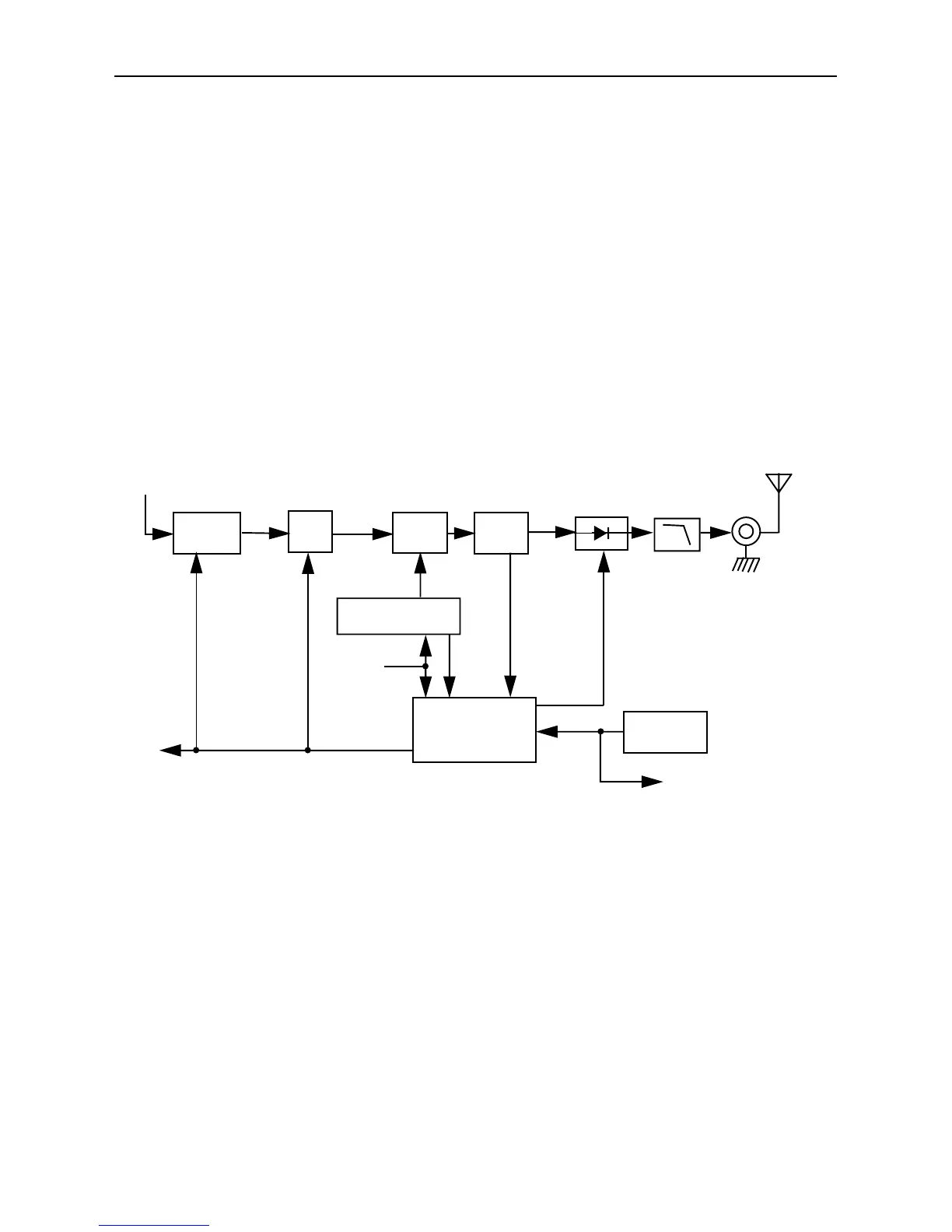
3.0 VHF (136-174MHz) Transmitter Power Amplifier (PA) 25 W
The radio’s 25 W PA is a three stage amplifier used to amplify the output from the VCOBIC to the
radio transmit level. All three stages utilize LDMOS technology. The gain of the first stage (U3401)
and the second stage (Q3421) is adjustable, controlled by pin 4 of PCIC (U3501) via U3402-1 and
U3402-2. It is followed by an LDMOS final stage (Q3441).
Figure 2-1 VHF Transmitter Block Diagram
Devices U3401, Q3421 and Q3441 are surface mounted. A pressure pad between board and the
radio's cover provides good thermal contact between the devices and the chassis.
3.1 First Power Controlled Stage
The first stage (U3401) is a 20dB gain integrated circuit containing two LDMOS FET amplifier
stages. It amplifies the RF signal from the VCO (TXINJ). The output power of stage U3401 is
controlled by a DC voltage applied to pin 1 from the op-amp U3402-1, pin 1. The control voltage
simultaneously varies the bias of two FET stages within U3401. This biasing point determines the
overall gain of U3401 and therefore its output drive level to Q3421, which in turn controls the output
power of the PA.
PCIC
Pin Diode
Antenna
Switch
RF Jack
Antenna
Harmonic
Filter
Power
Sense
PA-Final
Stage
From VCO
Controlled
Stage
Controlvoltage
Bias 2
To Microprocessor
Temperature
Sense
SPI BUS
ASFIC_CMP
PA
PWR
SET
To Microprocessor
PA
Driver

 Loading...