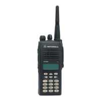
)
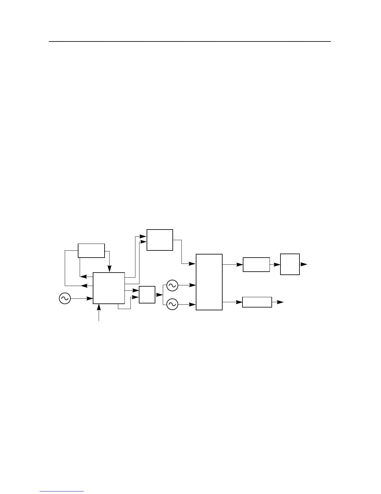
The frequency generation circuit, shown in Figure 2-3, is composed of Fractional-N synthesizer
U201 and VCO/Buffer IC U241. Designed in conjunction to maximize compatibility, the two ICs
provide many of the functions that normally require additional circuitry. The synthesizer block
diagram illustrates the interconnect and support circuitry used in the region. Refer to the schematic
for the reference designator.
The synthesizer is powered by regulated 5V and 3.3V which are provided by ICs U247 and U248
respectively. The 5V signal goes to pins 13 and 30 while the 3.3V signal goes to pins 5, 20, 34 and
36 of U201. The synthesizer in turn generates a superÞltered 5V which powers U241.
In addition to the VCO, the synthesizer also interfaces with the logic and ASFIC circuitry.
Programming for the synthesizer is accomplished through the data, clock and chip select lines (pins
7, 8 and 9) from the microprocessor, U409. A 3.3V dc signal from pin 4 indicates to the
microprocessor that the synthesizer is locked.
Transmit modulation from the ASFIC is supplied to pin10 of U201. Internally the audio is digitized by
the Fractional-N and applied to the loop divider to provide the low-port modulation. The audio runs
through an internal attenuator for modulation balancing purposes before going out at pin 41 to the
VCO.
 Loading...