Do you have a question about the Motorola Professional GP340 and is the answer not in the manual?
Information and instructions for the safe and efficient operation of Motorola Portable Two-Way Radios.
Guidelines for occupational use, informing users about RF energy exposure and control.
FCC rules for RF exposure limits and user awareness for occupational requirements.
Procedures for controlling occupational RF exposure and ensuring compliance with limits.
Recommendations for maintaining separation between radios and pacemakers for safe operation.
Guidelines for safe radio use while driving, emphasizing attention to the road.
Warning about placing radios in air bag deployment areas due to inflation force.
Warning to turn off radios in potentially explosive atmospheres unless certified intrinsically safe.
Warning to turn off radios near blasting caps or in blasting areas.
Cautions for operating intrinsically safe equipment in hazardous atmospheres.
Warnings related to shipping, modifications, and use of intrinsically safe radios.
Guidance on using approved system components to maintain intrinsic safety certification.
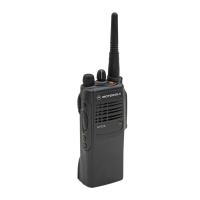
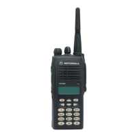
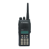
Details of the GP340 model, including specifications and required items.
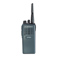
Details of the GP640/GP680 models, including specifications and required items.
General and specific technical data for the radios, including dimensions and battery life.
Overview of the chapter's content covering 300-350MHz circuits.
Detailed theory of operation for the transmitter circuits.
Explanation of the power amplifier's function and components.
Description of the antenna switch circuit's operation in transmit and receive modes.
Explanation of the harmonic filter's design and function for attenuating unwanted frequencies.
Description of the antenna matching network's role in optimizing performance.
Explanation of the PCIC's function in regulating transmitter output power.
Overview of the receiver's function, front end, back end, and AGC circuits.
Detailed explanation of the receiver's front-end circuitry and signal path.
Explanation of the front-end AGC circuit's function and components for gain reduction.
Overview of the circuitry responsible for generating frequencies.
Detailed explanation of the Fractional-N synthesizer and its components.
Explanation of the VCOBIC's role in generating RF signals for receive and transmit modes.
Step-by-step guide for troubleshooting receiver issues.
Continuation of the receiver troubleshooting flow chart.
Step-by-step guide for troubleshooting transmitter issues.
Step-by-step guide for troubleshooting synthesizer issues.
Step-by-step guide for troubleshooting VCO issues.
Allocation of schematics and circuit boards for controller and 300R1 components.
Information on controller circuits and their corresponding schematics and parts lists.
Component layout diagram for PCB 8485726Z01.
Schematic for the radio's controls and switches, including buttons and connectors.
Schematic diagram for the 300R1 receiver front-end components.
Schematic diagram for the 300R1 receiver back-end components.
Schematic diagram for the 300R1 synthesizer circuit.
Schematic diagram for the 300R1 voltage controlled oscillator circuit.
Schematic diagram for the 300R1 transmitter circuit.
Detailed list of parts for PCB 8485726Z01.
Defines the manual's purpose and intended audience.
Information on Motorola's product support, including exchange and repair services.
Details on warranty terms, conditions, and return procedures for product service.
Information on Motorola's support services available after the warranty period expires.
Contact information for Motorola's European Repair and Service Centre.
Information on ordering replacement parts and spare parts directly from Motorola.
Information on Motorola Product Services availability for resolving malfunctions.
List of documents directly related to the product's use and maintainability.
Overview of the chapter's topics: preventive maintenance, CMOS handling, and repair procedures.
Recommendations for periodic visual inspection and cleaning of the radio.
Guidance on checking external surfaces and controls for functionality and cleanliness.
Procedures for cleaning external plastic surfaces and internal circuit boards using recommended agents.
Precautions for preventing damage to CMOS and LDMOS devices during disassembly and repair.
Guidelines for replacing damaged parts with identical components or proper Motorola part numbers.
Guidelines for replacing damaged parts with identical components or proper Motorola part numbers.
Considerations for soldering and unsoldering components on multi-layer printed circuit boards.
Techniques for soldering flexible circuits, emphasizing avoiding excessive heat and bending.
Procedures for removing and replacing chip components using hot-air or soldering iron stations.
Procedures for removing and replacing shields using a R1070 station.
List of service aids recommended for radio maintenance and testing.
List of recommended tools for radio maintenance, including disassembly tools and soldering equipment.
List of test equipment required for servicing radios, including analyzers and oscilloscopes.
Allocation of schematics and circuit boards for flexible connectors and keypads.
Allocation of schematics for Keypad/Controller Flex and Universal Flex connectors.
Allocation of schematics and parts lists for standard and GP1280 keypads.
Schematic diagram for the Keypad/Controller Interconnect Flex.
Schematic diagram for the Universal Flex connector.
Layout diagrams for the standard keypad PCB (8480574Z06).
Schematic diagram for the standard keypad PCB (8480574Z06).
Parts list for the standard keypad PCB (8480574Z06).
Overview of the chapter covering power distribution and controller circuits.
Explanation of the DC power distribution throughout the radio board.
Description of the controller board as the central interface for radio subsystems.
Description of the controller board's architecture, separating MCU digital and audio/signalling.
Details of the digital architecture, including microcontroller, EEPROM, RAM, and ROM.
Explanation of the Real Time Clock (RTC) module for message time stamping and time keeping.
Information on the supply variations to the ModB/Vstby pin based on conditions.
Explanation of the audio/signalling/filter/companding IC and audio power amplifier components.
Troubleshooting chart for the 300R1 controller issues.
Troubleshooting chart for VHF controllers, excluding specific PCB models.
Troubleshooting chart for VHF controllers specifically for models with PCB 8486473Z04.
Troubleshooting chart for lowband controller issues.
Allocation of schematics and circuit boards for controller circuits.
Details on controller circuit schematics and PCB component layouts for lowband.
Information on the voice storage facility and its schematics.
Overall controller schematic for Set 1 PCBs.
Schematic diagram for the controller's ASIC and ON/OFF circuitry.
Schematic diagram for the controller's microprocessor.
Schematic diagram for the controller interface.
Schematic diagram for the controller memory components.
Overall controller schematic for Set 2 PCBs.
Schematic diagram for the controller's ASIC and ON/OFF circuitry.
Schematic diagram for the controller memory components.
Schematic diagram for the controller's microprocessor.
Schematic diagram for the controller interface.
Schematic diagram for the controller's audio power amplifier.
Overall controller schematic for Set 3 PCBs.
Schematic diagram for the controller's ASIC and ON/OFF circuitry.
Schematic diagram for the controller's microprocessor.
Schematic diagram for the controller interface.
Schematic diagram for the controller memory components.
Overall controller schematic for Set 4 PCBs.
Schematic diagram for the controller's ASIC and ON/OFF circuitry.
Schematic diagram for the controller's microprocessor.
Schematic diagram for the controller interface.
Schematic diagram for the controller memory components.
Overall controller schematic for Set 5 PCBs.
Schematic diagram for the controller's ASIC and ON/OFF circuitry.
Schematic diagram for the controller's microprocessor.
Schematic diagram for the controller interface.
Schematic diagram for the controller memory components.
Overall schematic for the controller, showing interconnections between major blocks.
Schematic diagram for the controller's ASIC and ON/OFF circuitry.
Schematic diagram for the controller's microprocessor.
Schematic diagram for the controller interface.
Schematic diagram for the controller memory components.
Model chart for GP320, GP340, GP360, GP380 series radios.
Model chart for the GP140 radio.
Model chart for the GP640 and GP680 radios.
Model chart for the GP1280 radio.
Model chart for GP240, GP280, GP540, GP580 series radios.
Detailed technical specifications for the VHF radios.
Introduction to the theory of operation for VHF circuits in the radio.
Detailed theory of operation for the VHF transmitter.
Explanation of the power amplifier's function and components.
Description of the antenna switch circuit's operation.
Explanation of the harmonic filter's design and function.
Description of the antenna matching network's role.
Explanation of the PCIC's function in regulating transmitter output power.
Detailed description of the VHF receiver's front end, back end, and AGC circuits.
Explanation of the VHF receiver's front-end circuitry.
Detailed description of the VHF receiver's front end, back end, and AGC circuits for specific PCB models.
Explanation of the VHF receiver's front-end circuitry for specific PCB models.
Explanation of the frequency generation circuitry.
Detailed explanation of the Fractional-N synthesizer.
Explanation of the VCO's function and components.
Explanation of the voice storage feature and its audio path.
Step-by-step guide for troubleshooting receiver issues, excluding specific PCB models.
Continuation of receiver troubleshooting for specific PCB models.
Step-by-step guide for troubleshooting receiver issues for models with PCB 8486473Z04.
Continuation of receiver troubleshooting for specific PCB models.
Step-by-step guide for troubleshooting transmitter issues.
Step-by-step guide for troubleshooting synthesizer issues.
Step-by-step guide for troubleshooting VCO issues.
Troubleshooting chart for issues related to receiving messages and personal memo recording.
Troubleshooting chart for issues related to message playback.
Allocation of schematics and circuit boards for VHF circuits.
Details on controller circuit schematics and PCB component layouts.
Information on the voice storage facility and its schematics.
Component layout diagram for VHF PCB 8486062B12.
Schematic diagram for the VHF receiver front-end components.
Schematic diagram for the VHF receiver back-end components.
Schematic diagram for the VHF synthesizer circuit.
Schematic diagram for the VHF voltage controlled oscillator circuit.
Schematic diagram for the VHF transmitter circuit.
Detailed list of parts for VHF PCB 8486062B12.
Component layout diagram for VHF PCB 8486101B09.
Schematic diagram for the GP1280 voice storage feature.
Top side component layout for VHF PCB 8486101B10.
Bottom side component layout for VHF PCB 8486101B10.
Detailed list of parts for VHF PCB 8486062B16.
Detailed list of parts for VHF PCB 8486062B16.
Detailed list of parts for VHF PCB 8486062B16.
Component layout diagram for VHF PCB 8486062B16.
Detailed list of parts for VHF PCB 8486062B17.
Detailed list of parts for VHF PCB 8486062B17.
Component layout diagram for VHF PCB 8486062B16.
Bottom side component layout for VHF PCB 8486062B16.
Schematic diagram for VHF controls and switches.
Schematic diagram for the VHF receiver front-end.
Schematic diagram for the VHF receiver back-end.
Schematic diagram for the VHF synthesizer.
Schematic diagram for the VHF voltage controlled oscillator.
Schematic diagram for the VHF transmitter.
Detailed list of parts for VHF PCB 8486062B16.
Detailed list of parts for VHF PCB 8486062B16.
Detailed list of parts for VHF PCB 8486062B16.
Detailed list of parts for VHF PCB 8486062B16.
Component layout diagram for VHF PCB 8486062B16.
Bottom side component layout for VHF PCB 8486062B16.
Detailed list of parts for VHF PCB 8486101B11.
Detailed list of parts for VHF PCB 8486101B11.
Detailed list of parts for VHF PCB 8486101B11.
Component layout diagram for VHF PCB 8486101B11.
Detailed list of parts for VHF PCB 8486101B11.
Detailed list of parts for VHF PCB 8486101B11.
Detailed list of parts for VHF PCB 8486101B11.
Component layout diagram for VHF PCB 8486473Z04.
Schematic diagram for VHF controls and switches.
Schematic diagram for the VHF receiver front-end.
Schematic diagram for the VHF receiver back-end.
Schematic diagram for the VHF synthesizer.
Schematic diagram for the VHF voltage controlled oscillator.
Schematic diagram for the VHF transmitter.
Detailed list of parts for VHF PCB 8486473Z04.
Detailed list of parts for VHF PCB 8486473Z04.
Model chart for GP340/GP380 series radios.
Technical specifications for the lowband radios.
Introduction to the theory of operation for lowband RF circuits.
Detailed theory of operation for the lowband transmitter.
Explanation of the power amplifier's function and components.
Description of the antenna switch circuit's operation.
Explanation of the harmonic filter's design and function.
Description of the antenna matching network's role.
Explanation of the PCIC's function in regulating transmitter output power.
Detailed description of the lowband receiver's stages.
Explanation of the lowband receiver's front-end circuitry.
Explanation of the frequency generation circuitry.
Detailed explanation of the Fractional-N synthesizer.
Step-by-step guide for troubleshooting receiver issues (Sheet 1 of 2).
Continuation of receiver troubleshooting (Sheet 2 of 2).
Troubleshooting chart for transmitter issues.
Troubleshooting chart for synthesizer issues.
Troubleshooting chart for VCO issues.
Allocation of schematics and circuit boards for lowband controller circuits.
Details on controller circuit schematics and PCB component layouts for lowband.
Component layout diagram for Lowband PCB 8485658Z03.
Overall schematic diagram for the lowband receiver.
Schematic diagram for the lowband receiver front-end.
Schematic diagram for the lowband receiver back-end.
Schematic diagram for the lowband synthesizer.
Schematic diagram for the lowband voltage controlled oscillator.
Schematic diagram for the lowband transmitter.
Detailed list of parts for Lowband PCB 8485658Z03.
Detailed list of parts for Lowband PCB 8485658Z03.
Detailed list of parts for Lowband PCB 8485658Z03.
| Channel Capacity | 16 channels |
|---|---|
| Dimensions | 137 x 57.5 x 37.5 mm |
| IP Rating | IP54 |
| Operating Temperature | -30°C to +60°C |
| Frequency Range | 136-174 MHz (VHF), 403-470 MHz (UHF) |
| Power Output | 1-5W (VHF), 1-4W (UHF) |
| Power Supply | 7.5V |
| Battery Life | up to 11 hours (with standard battery) |
| Weight | 420g (with standard NiMH battery) |