Chapter 2
THEORY OF OPERATION
1.0 Introduction
This chapter provides a detailed theory of operation for the radio RF circuits. Refer to the relevant
section of this manual for details of the operation of the Controller Circuits.
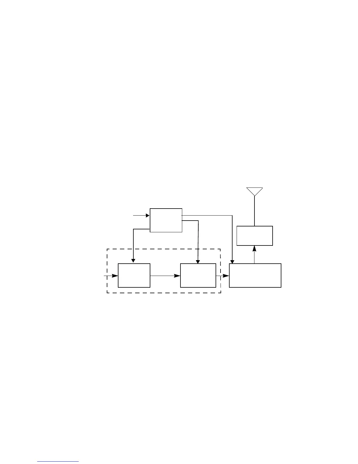
2.0 Lowband Transmitter
(
Refer to Figure 2-1 and the Lowband Transmitter schematic diagram
)
The Lowband transmitter consists of the following basic circuits :
■ Power amplifier (PA).
■ Antenna switch/harmonic filter.
■ Antenna matching network.
■ Power Control Integrated Circuit (PCIC).
Figure 2-1 Lowband Transmitter Block Diagram.
2.1 Power Amplifier (PA)
The power amplifier (PA) consists of two LDMOS devices:
1. PA driver IC, U101.
2. PA final stage, Q100.
The LDMOS driver (U101) provides 2-stage amplification using a supply voltage of 7.3V. The
amplifier is capable of supplying an output power of 0.3W (pins 6 and 7) with an input signal of 2mW
at (pin16). The current drain is typically 120mA while operating in the frequency range of
29.7 - 50 MHz. The power output of this stage is varied by the power control loop which controls the
voltage on pin 1.
PCIC
SPI Bus
Antenna switch bias
V Control
Power Amplifier (PA)
PA Driver
PA Final
Stage
Antenna Switch/
Harmonic Filter
Antenna
Matching
Network
Gate bias
 Loading...