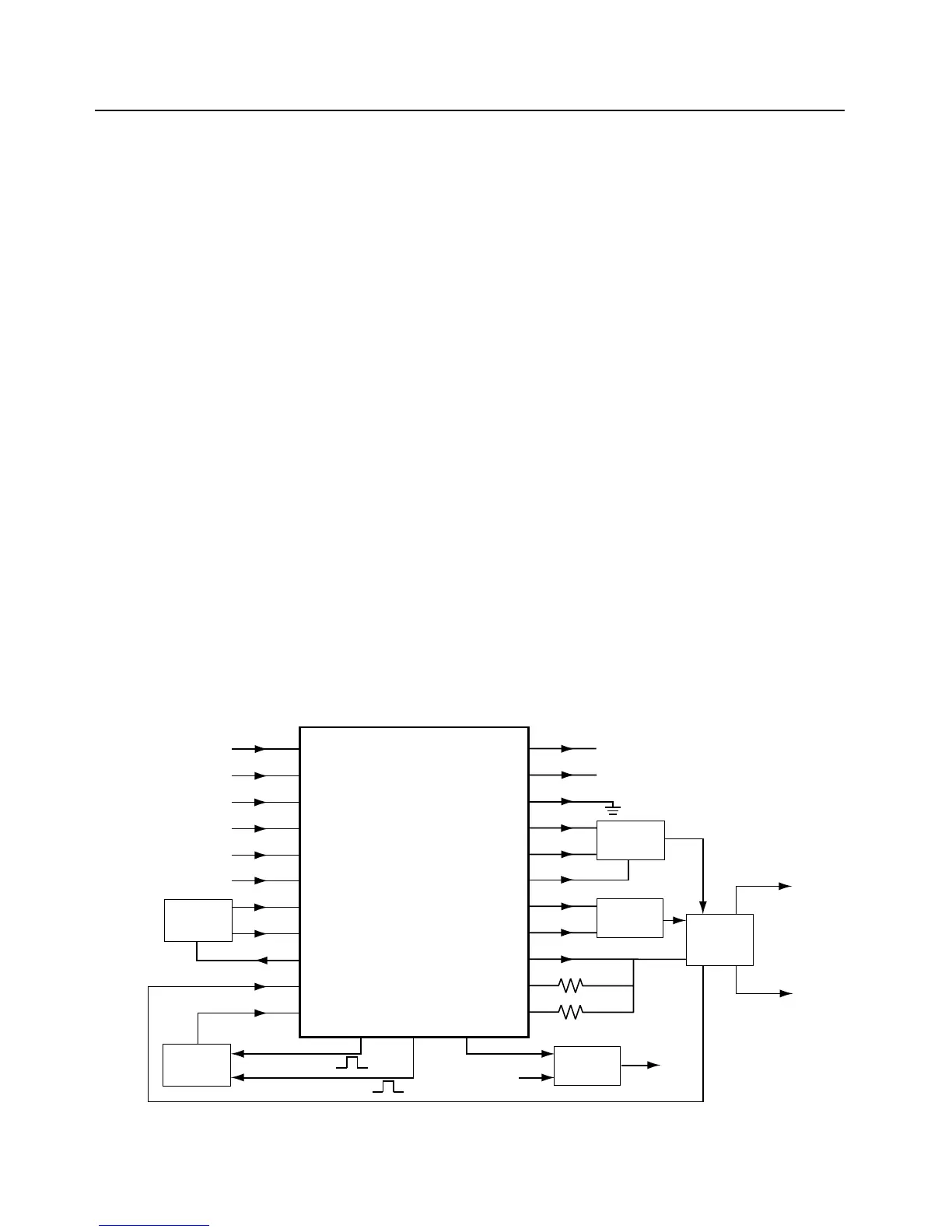
7-12 Low Band, 800 MHz, PassPort & 900 MHz Theory of Operation: Synthesizer
Transmit modulation from the ASFIC is supplied to pin10 of U201. Internally the audio is digitized by
the Low Voltage Fractional-N synthesizer and applied to the loop divider to provide the low-port
modulation. The audio runs through an internal attenuator for modulation balancing purposes before
going out to the VCO.
7.8 Synthesizer
The Low Voltage Fractional-N (LV FracN) synthesizer (U201) shown in Figure 7-8 on page 7-12
uses a 16.8 MHz crystal (FL201) to provide a reference for the system. The LV FracN IC further
divides this to 2.1 MHz, 2.225 MHz, and 2.4 MHz as reference frequencies. Together with C235,
C236, C237, R211 and CR203, they comprise the reference oscillator which is capable of 2.5ppm
stability over temperatures of -30° to 85°C. It also provides 16.8 MHz at pin 19 of U201 to be used by
ASFIC and LVZIF.
Some models are equipped with a packaged 1.5ppm reference oscillator, Y200. On these models
components C235, C236, C237, CR203, FL201, and R211 are not placed. Components C238,
C239, C241, R212, R213, R214 and Y200 are placed instead.
The loop filter which consists of C220, C225, C226, R204, R209 and R210 provides the necessary
dc steering voltage for the VCO and provides filtering of noise and spurs from U201.
In achieving fast locking for the synthesizer, an internal adapt charge pump provides higher current
at pin 45 of U201 to put the synthesizer within the lock range. The required frequency is then locked
by the normal mode charge pump at pin 43.
Both the normal and adapt charge pumps get their supply from the capacitive multiplier which is
made up of D201, D202, C244, C245, C246, C247, R200, R218, C208, C243, R219, and R220. Two
3.3 V square waves (180 degrees out of phase) are applied to R219 and R220. These square waves
switch alternate sets of diodes from D201 and D202, which in turn charge C244, C245, C246, and
C247 in a bucket brigade fashion. The resulting output voltage that is applied to pin 47 of U201 is
typically 12.8 V and allows the steering line voltage (VCO control voltage) to reach 11 V.
Figure 7-8. 800 MHz Synthesizer Block Diagram
DATA
CLK
CEX
MODIN
V
CC
, DC5V
XTAL1
XTAL2
WARP
PREIN
VCP
Reference
Oscillator
Voltage
Multiplier
Voltage
Controlled
Oscillator
2-Pole
Loop Filter
DATA (U409 Pin 100)
CLOCK (U409 Pin 1)
CSX (U409 Pin 2)
MOD IN (U404 Pin 40)
+5V (U247 Pin 4)
7
8
9
10
13,30
23
24
25
32
47
VMULT2
VMULT1
BIAS1
SFOUT
AUX3
AUX4
IADAPT
IOUT
GND
FREFOUT
LOCK
4
19
6,22,23,24
43
45
3
2
28
14
15
40
Filtered 5V
12.8V
3.3Vp-p
3.3Vp-p
Steering
Line
11.0V
LOCK (U409 Pin 56)
Prescaler In
LO RF
Injection
TX RF
Injection
(First Stage of PA)
FREF (U201 Pin 21 & U404 Pin 34)
39
BIAS2
41
Dual
Transistors
48
5V
R405
(U248 Pin 5)
AUX1
V
DD
, 3.3V
MODOUT
U251
Low Voltage
Fractional-N
Synthesizer
5,20,34,36
Dual
Transistors
 Loading...