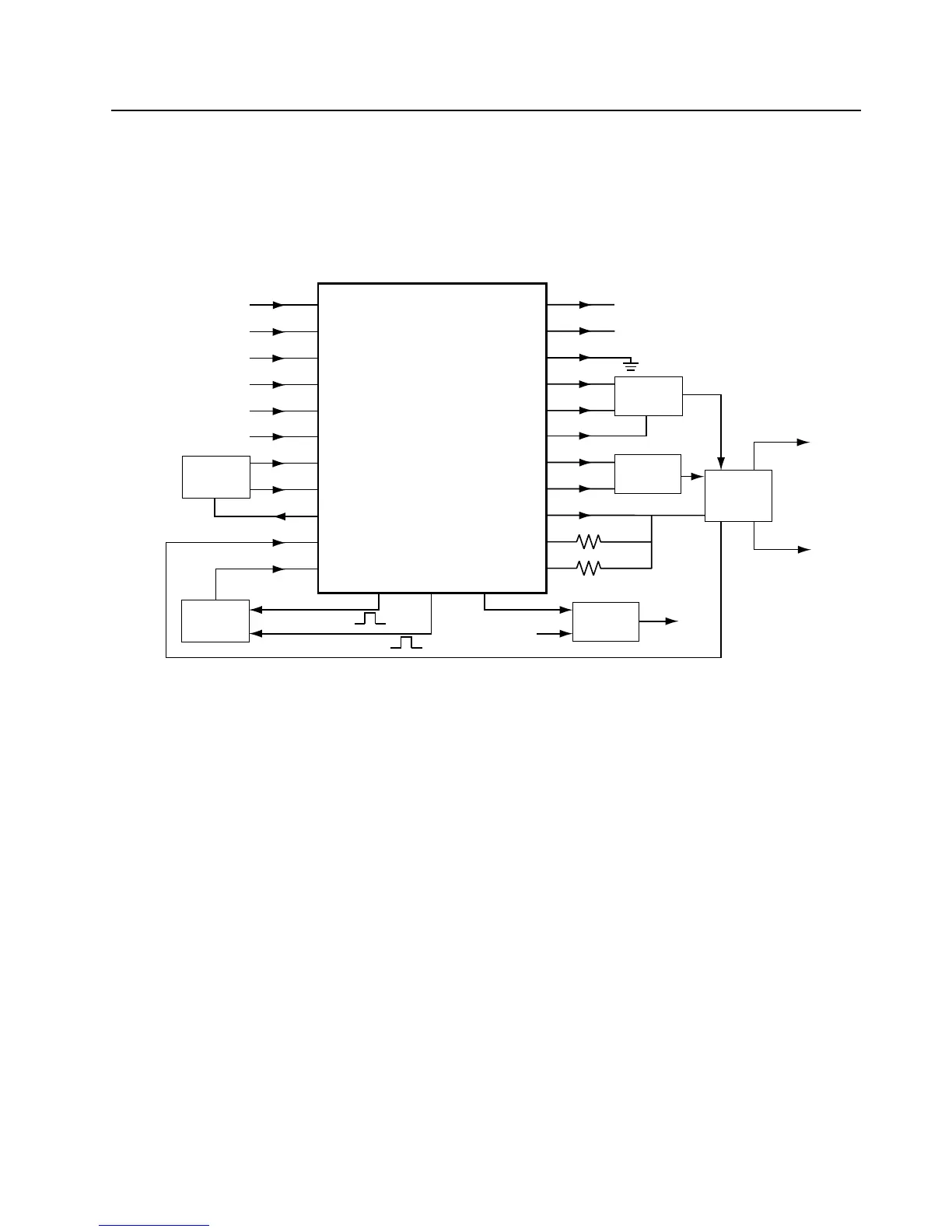
Low Band, 800 MHz, PassPort & 900 MHz Theory of Operation: 900 MHz Synthesizer 7-23
Both the normal and adapt charge pumps get their supply from the capacitive multiplier which is
made up of CR201, CR202, C244, C245, C246, C247, R200, R218, C208, C243, R219, and R220.
Two 3.3 V square waves (180 degrees out of phase) are applied to R219 and R220. These square
waves switch alternate sets of diodes from CR201 and CR202, which in turn charge C244, C245,
C246, and C247 in a bucket brigade fashion. The resulting output voltage that is applied to pin 47 of
U201 is typically 12.8 V and allows the steering line voltage (VCO control voltage) to reach 11 V.
Figure 7-13. Synthesizer Block Diagram
DATA
CLK
CEX
MODIN
V
CC
, DC5V
XTAL1
XTAL2
WARP
PREIN
VCP
Reference
Oscillator
Voltage
Multiplier
Voltage
Controlled
Oscillator
2-Pole
Loop Filter
DATA (U409 Pin 100)
CLOCK (U409 Pin 1)
CSX (U409 Pin 2)
MOD IN (U404 Pin 40)
+5V (U247 Pin 4)
7
8
9
10
13,30
23
24
25
32
47
VMULT2
VMULT1
BIAS1
SFOUT
AUX3
AUX4
IADAPT
IOUT
GND
FREFOUT
LOCK
4
19
6,22,23,24
43
45
3
2
28
14
15
40
Filtered 5V
12.8V
3.3Vp-p
3.3Vp-p
Steering
Line
11.0V
LOCK (U409 Pin 56)
Prescaler In
LO RF
Injection
TX RF
Injection
(First Stage of PA)
FREF (U201 Pin 21 & U404 Pin 34)
39
BIAS2
41
Dual
Transistors
48
5V
R405
(U248 Pin 5)
AUX1
V
DD
, 3.3V
MODOUT
U251
Low Voltage
Fractional-N
Synthesizer
5,20,34,36
Dual
Transistors
 Loading...