Notice
LLM 21 2.0g1.25
(in mm)
Chip
(LgW)
0.6 to 0.8
a
(0.3 to 0.5)
b, b'
0.3
c, c'
2.0 to 2.6
d
1.3 to 1.8
e
1.4 to 1.6
f
0.5
p
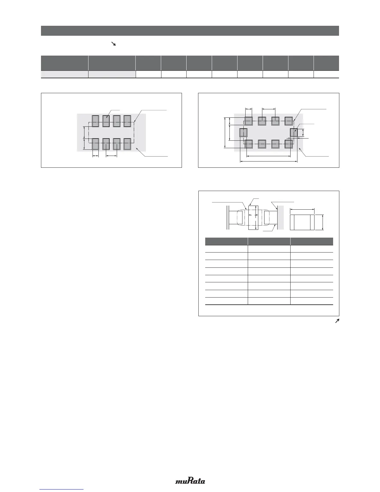
Table 5 LLM Series Reflow Soldering Method
b=(c-e)/2, b'=(d-f)/2
[Land for LLA Series] [Land for LLM Series]
c'
a
e
b
c p
f
b'
d
Solder Resist Solder Resist
pc
ab
Chip Capacitor
Chip Capacitor
Land
Land
2-2. Dimensions of Slit (Example)
Preparing the slit helps flux cleaning and resin
coating on the back of the capacitor.
However, the length of the slit design should be as
short as possible to prevent mechanical damage in
the capacitor.
A longer slit design might receive more severe
mechanical stress from the PCB.
Recommended slit design is shown in the Table.
1.6g0.8
2.0g1.25
3.2g1.6
3.2g2.5
4.5g2.0
4.5g3.2
5.7g2.8
5.7g5.0
–
–
1.0 to 2.0
1.0 to 2.0
1.0 to 2.8
1.0 to 2.8
1.0 to 4.0
1.0 to 4.0
–
–
3.2 to 3.7
4.1 to 4.6
3.6 to 4.1
4.8 to 5.3
4.4 to 4.9
6.6 to 7.1
LgWd e
(in mm)
<Applicable to beyond Rated Voltage of 200VDC>
Land
Solder Resist
L
W
Chip Capacitor
Slit
d
e
Series
Chip Dimension Code
(L/W)
Continued from the preceding page.
Continued on the following page.
!
Note
• Please read rating and
!
CAUTION (for storage, operating, rating, soldering, mounting and handling) in this catalog to prevent smoking and/or burning, etc.
• This catalog has only typical specifications. Therefore, please approve our product specifications or transact the approval sheet for product specifications before ordering.