REF10
NANO
16
Appendix
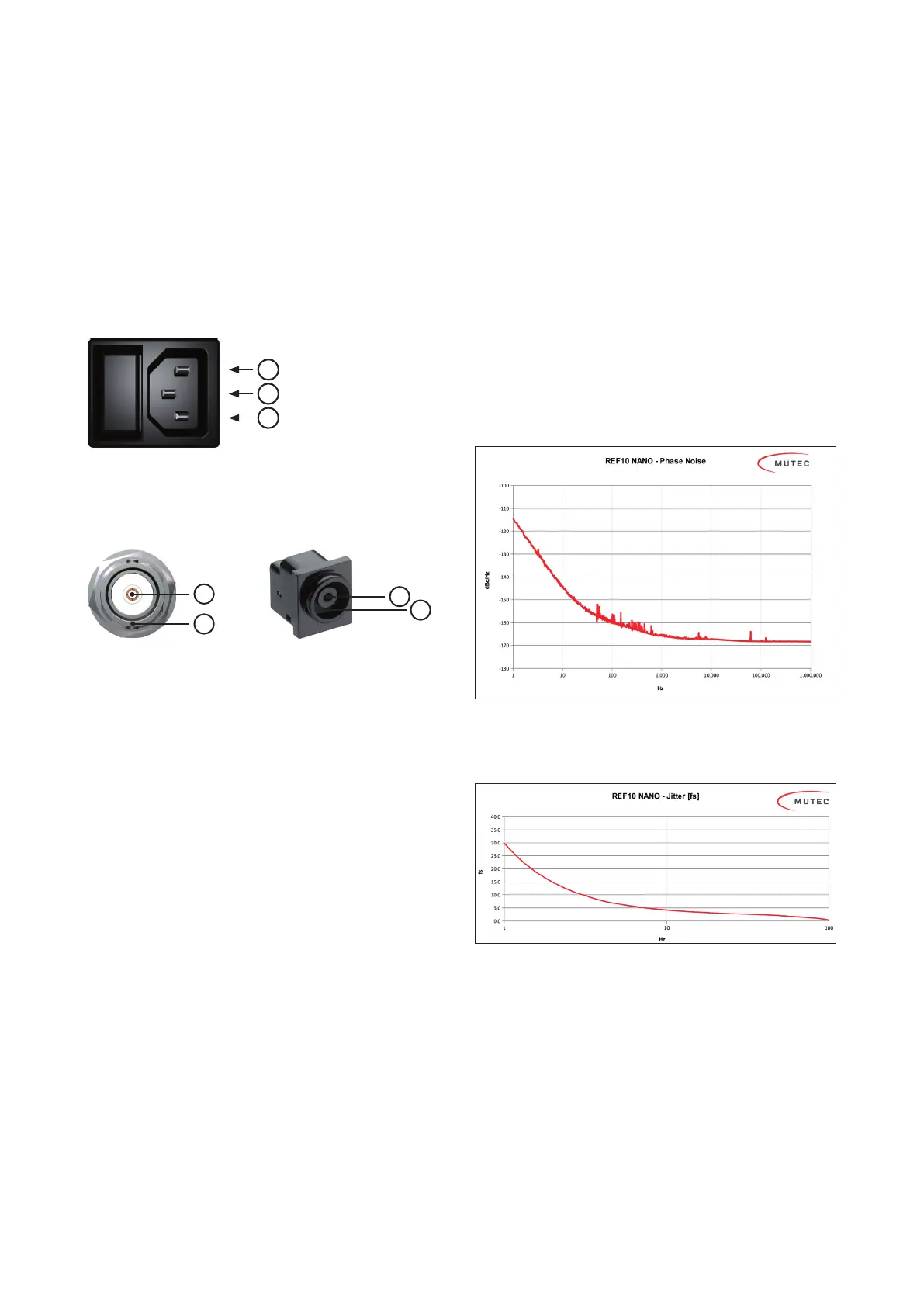
Pin Assignment of the Terminals
Mains
1) Neutral (N)
2) Protective Earth (E)
3) Live, Phase (P)
Technical Data
Clock Outputs:
•
2 x BNC, unbalanced, 50 terminated, galvanically
isolated, buffert
•
2 x BNC, unbalanced, 75 terminated, galvanically
isolated, buffert
Clock Signal Format of all Outputs
•
Square wave, 10.000 MHz, ≈2 Vpp, ≈1 V RMS,
50:50 duty cycle
Clock Generation:
•
Type: 10.000 MHz low phase noise oven-controlled crystal
oscillator
•
Frequency accuracy when shipped: < ±0.01 ppm
•
Frequency stability vs. temperature range: < ±0.01 ppm
within -20 °C to +70 °C (-4 °F to +158 °F)
•
Short term stability (Allan Deviation, typically Tau = 1s):
2 × 10
-12
•
Aging after 30 days operation: : < +/-0.0002 ppm (per
day), < +/-0.03 ppm (first year), < +/-0.2 ppm (ten years)
•
Warm-up time at +25 °C (+77 °F): <5 min
Phase Noise measured at REF10 NANO's Clock Outputs (!):
•
1 Hz: ≤ -112 dB/c
•
10 Hz: ≤ -142 dB/c
•
100 Hz: ≤ -158 dB/c
•
1000 Hz: ≤ -164 dB/c
•
Noise Floor: ≤ -167 dB/c
Jitter measured at REF10 NANO's Clock Outputs (!):
•
1-100 Hz: ≈30 fs
(Disclaimer: All measurement figures represent average values. Minor pro-
duction related deviations will be expected.)
Mains Power Supply:
•
Type: internal, self-switching power supply
•
Input voltages: 85-305 V, 50-60 Hz
•
Power consumption: 7 W during oscillator warm-up,
4 W nominal operation (all outputs terminated)
BNC Output 50/75 Ω DC Power Input
1) Signal
2) Ground
1) Signal
2) Ground
1
2
3
2
1
1
2