Appendix B Timing Diagrams
© National Instruments Corporation B-21 M Series User Manual
Analog Output Timing Diagrams
The analog output timing can be broken into the following three sections:
• Input Timing—The timing for external signals to enter the M Series
device and be available on the internal signal buses
• Internal Analog Output Timing—The timing specifications of the
analog output unit itself, to and from internal signals
• Output Timing—The timing of exported signals going to the M Series
device external terminals
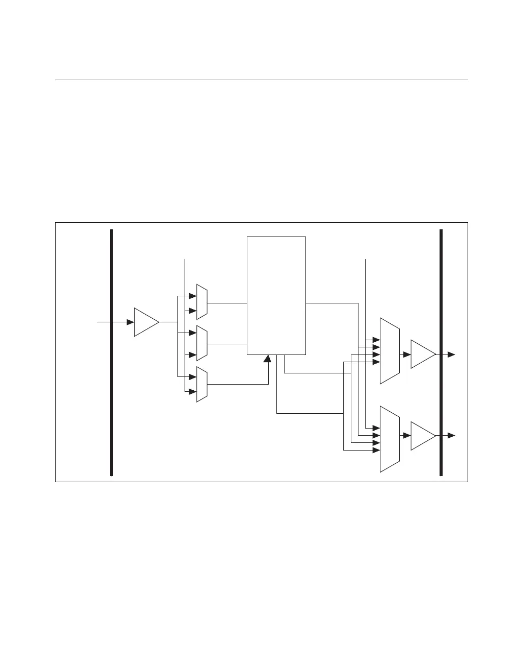
Figure B-22 gives an overview of analog output timing.
Figure B-22. M Series Analog Output Timing
The following signals are used in Figure B-22 and in the following
sections:
• Sample Clock—This signal multiplied by the digital to analog
conversions. This signal is routed to the DAC, and in every pulse, the
DAC will perform a data conversion. This signal can come directly
from an external signal or can be the result of dividing down the
Sample Clock Timebase using the UI counter.
STAR_TRIG,
RTSI, or
PFI
STAR_TRIG_i,
RTSI_i, or
PFI_i
Internal
Sources
Sample
Clock
Timebase
Selected Pause
Selected
STA R T
Other
Internal
Sources
PFI
RTSI
Pause Trigger
START Trigger
Sample Clock
AO TIMER
 Loading...