Chapter 3 Signal Connections
© National Instruments Corporation 3-17 NI 660x User Manual
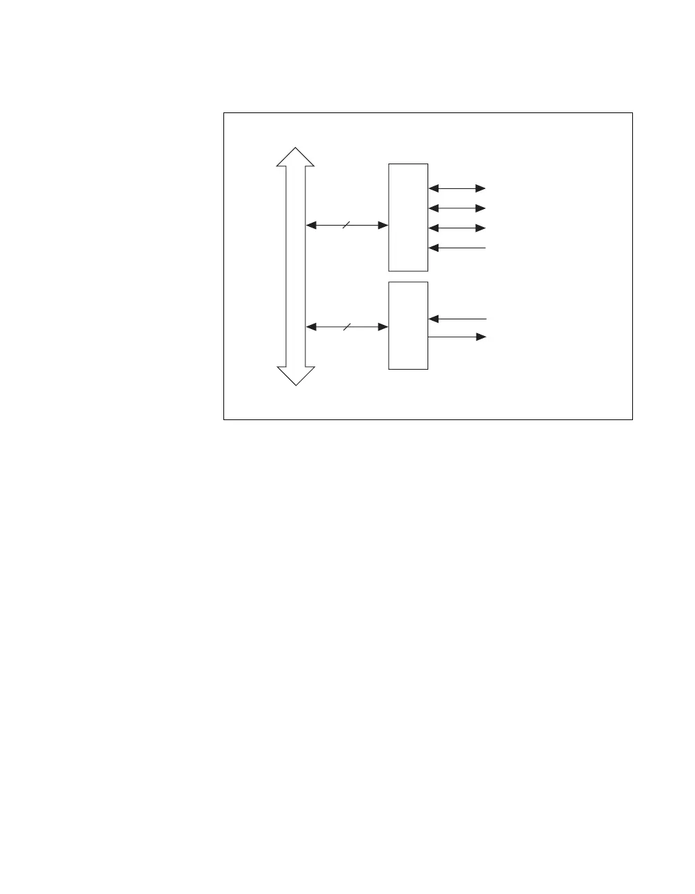
Figure 3-7 shows the RTSI signal connection scheme for PCI TIO devices.
Figure 3-7. RTSI Signal Connection Scheme for PCI
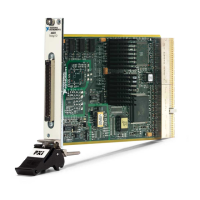
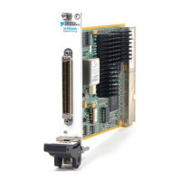
PXI TIO devices use PXI trigger line 7 as their RTSI clock line. The
maximum timebase provided by the PXI TIO device is phase locked to the
10 MHz PXI backplane clock. By using other PXI modules that phase lock
their board clocks to the 10 MHz PXI backplane clock, you can better
synchronize operation in a multi-module PXI system. The phase locking is
enabled by default and can be disabled by way of software. If the module
is used in a compact PCI chassis that does not have the 10 MHz PXI
backplane clock, the phase locking is automatically disabled. Additionally,
PXI trigger line 6 corresponds to PXI star trigger on PXI TIO devices.
Trigger <0..6>
Ctr
n
Source
Ctr
n
Gate
Ctr
n
Aux
Ctr
n
InternalOutput
20 MHz Timebase
Master Timebase
RTSI Trigger 7
RTSI Bus Connector
RTSI SwitchRTSI Switch
 Loading...