GeForce GTX 980 Whitepaper
GM204 HARDWARE ARCHITECTURE
IN-DEPTH
9
and power that had to be spent to manage data transfer in the more complex datapath organization
used by Kepler.
Compared to Kepler, the SMM’s memory hierarchy has also changed. Rather than implementing a
combined shared memory/L1 cache block as in Kepler SMX, Maxwell SMM units feature a 96KB
dedicated shared memory, while the L1 caching function has been moved to be shared with the texture
caching function.
As a result of these changes, each Maxwell CUDA core is able to deliver roughly 1.4x more performance
per core compared to a Kepler CUDA core, and 2x the performance per watt. At the SM level, with 33%
fewer total cores per SM, but 1.4x performance per core, each Maxwell SMM can deliver total per-SM
performance similar to Kepler’s SMX, and the area savings from this more efficient architecture enabled
us to then double up the total SM count, compared to GK104.
PolyMorph Engine 3.0
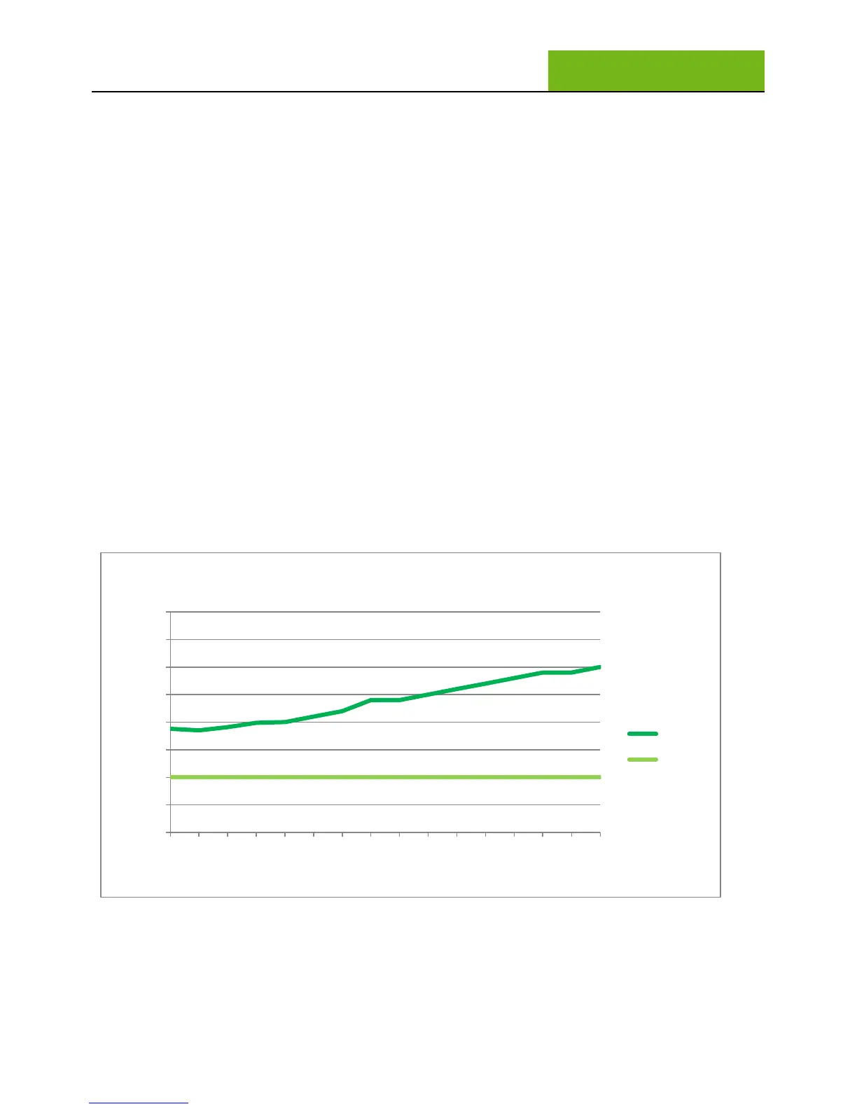
Tessellation was one of DirectX 11’s key features and will play a bigger role in the future as the next
generation of games are designed to use more tessellation. With the addition of more SMs in GM204,
GTX 980 also benefits from 2x the Polymorph Engines, compared to GTX 680. As a result, performance
on geometry heavy workloads is roughly doubled, and due to architectural improvements within the PE,
can achieve up to 3x performance improvement with high tessellation expansion factors.
0.0
0.5
1.0
1.5
2.0
2.5
3.0
3.5
4.0
1 3 5 7 9 11 13 15 17 19 21 23 25 27 29 31
Performance
Expansion Factor
Microsoft SubD11 SDK Test
GTX 980
GTX 680