FM Transmitter
Sistemas Electrónicos S.A EM 250 COMPACT DIG
Technical Manual - v1.1 - February 2006 33
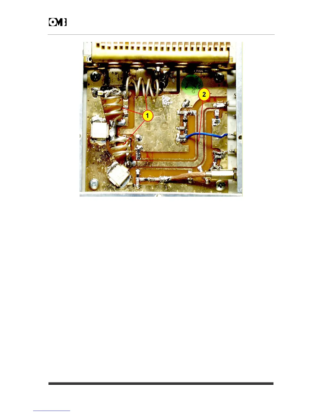
Fig. 2-6: DETAILED VIEW OF LOW-PASS FILTER and DIRECTIONAL COUPLER SECTION.
The three-section low-pass filter (1) attenuates the harmonics to a value that is generally below -70dBc,
following the output transistor drain circuit. Also, included in the RF output path, a directional coupler
(2) generates a dc signal, which is proportional to the forward and reflected RF power, and a RF non-
demodulated sample (RF MONITOR) to be externally used by a frequency counter or a modulation
monitor, for measurements purposes.
The transistor gate is biased by a Zener network and a resistor to set 50mA drain current, with 2.8Vgs.
Varying the control voltage towards a negative supply progressively disables the amplifier transistor,so
effectively acting as an AGC input. In fact the power management circuit, in a closed loop driven by
the output sensor circuitry, varies this voltage.This will accordingly vary the output power to obtain the
pre-set value and cope with alarm and start-up conditions.
The output transistors capsule is a rugged device which easily could pass the nominal 250W power
output, even increasing this power output out of limits, to 300W. OMB suggests never exceeding 250 ~
270W output power, even when the transmitter could generate more than this.