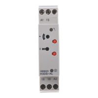
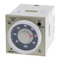
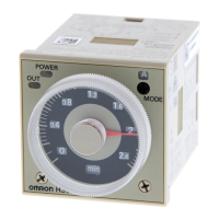
H5CN
H5CN
207
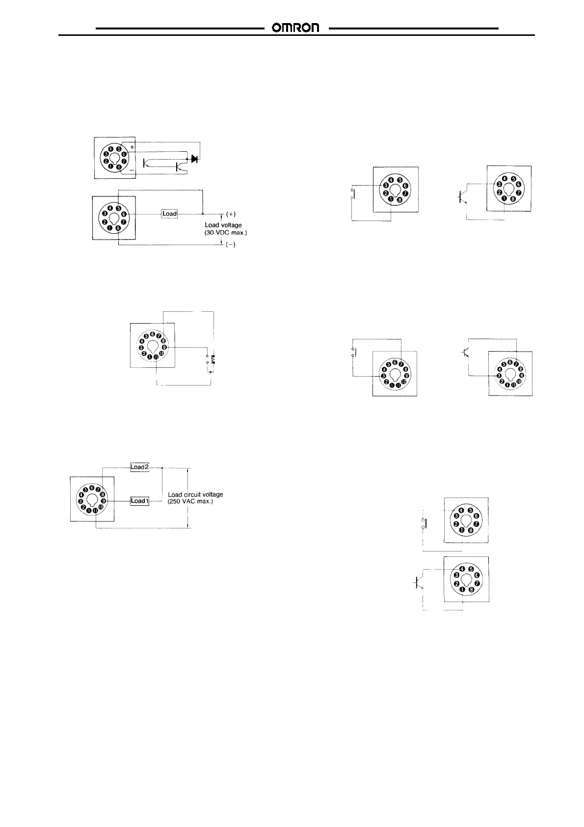
Solid-state Output Type (H5CN-
j
NS)
With H5CN-
j
NS, a solid-state output is generated by using an
open collector transistor. Connect terminal
F
(collector) of the timer
tothepositiveterminal of aloadandterminal
H
(emitter)to thenega-
tive terminal.
When connecting an inductive load to the timer, connect terminal
E
of the timer to the positive terminal of the loads, since a diode is in-
ternally connected between terminals
F
and
E
.
Model With Backup Power for Memory Protection
Contact Output Type
(Internal circuit of control output contact)
Terminal
H
,
I
, and
K
are for control output contacts.
(Connection of load circuit)
Load 1 connected in series with NO contact (between terminals
I
and
K
) is normally open, and the load circuit voltage will be applied
toitafterthelapseofthesettime.Theloadcircuitvoltageisnormally
applied to load
B
connected in series with NC contact (between ter-
minals
H
and
K
), which will be open after the lapse of the set time.
Note: The maximum load current is 3 A (resistive load).
Connection of Reset Input
Model Without Backup Power for Memory Protection
Connection of the reset input contact or an open collector transistor
between terminals
A
and
C
permits the timer to reset when contact
is made or the transistor turns ON. Use of a high-reliability gold-
plated contact is recommended for the reset input. For the reset in-
put transistor, select the one satisfying the following electrical rat-
ings:
V
CEO
=20Vmin.
IC = 50 mA min.
I
CBO
=0.5
&
Amax.
Reset input
contact
(Timer resets
when contact
is made.)
Reset input
transistor
(Timer resets
when transis-
tor is ON.)
Model With Backup Power for Memory Protection
Connection of the reset input contact or an open collector transistor
between terminals
C
and
G
permits the timer to reset when contact
is made or the transistor turns ON. Use of a high-reliability gold-
plated contact is recommended for the reset input. For the reset in-
put transistor, select the one satisfying the following electrical rat-
ings:
V
CEO
=20Vmin.
IC = 50 mA min.
I
CBO
=0.5
&
Amax.
Reset input
contact
(Timer resets
when contact
is made.)
Reset input
transistor
(Timer resets
when transis-
tor is ON.)
Connection of Gate Input
Model Without Backup Power for Memory Protection
Connection of the gate input contact or an open collector transistor
between terminals
A
and
C
permits the timer to reset when contact
is made or the transistor turns ON. Use of a high-reliability gold-
plated contact is recommended for the gate input. For the reset in-
put transistor, select the one satisfying the following electrical rat-
ings:
Gate input contact
(Timer stops when
contact is made.)
Gate input transistor
(Timer stops when
transistor is ON.)