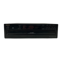
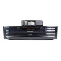
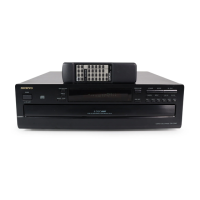
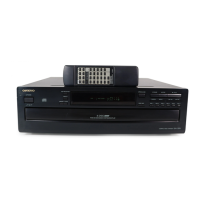
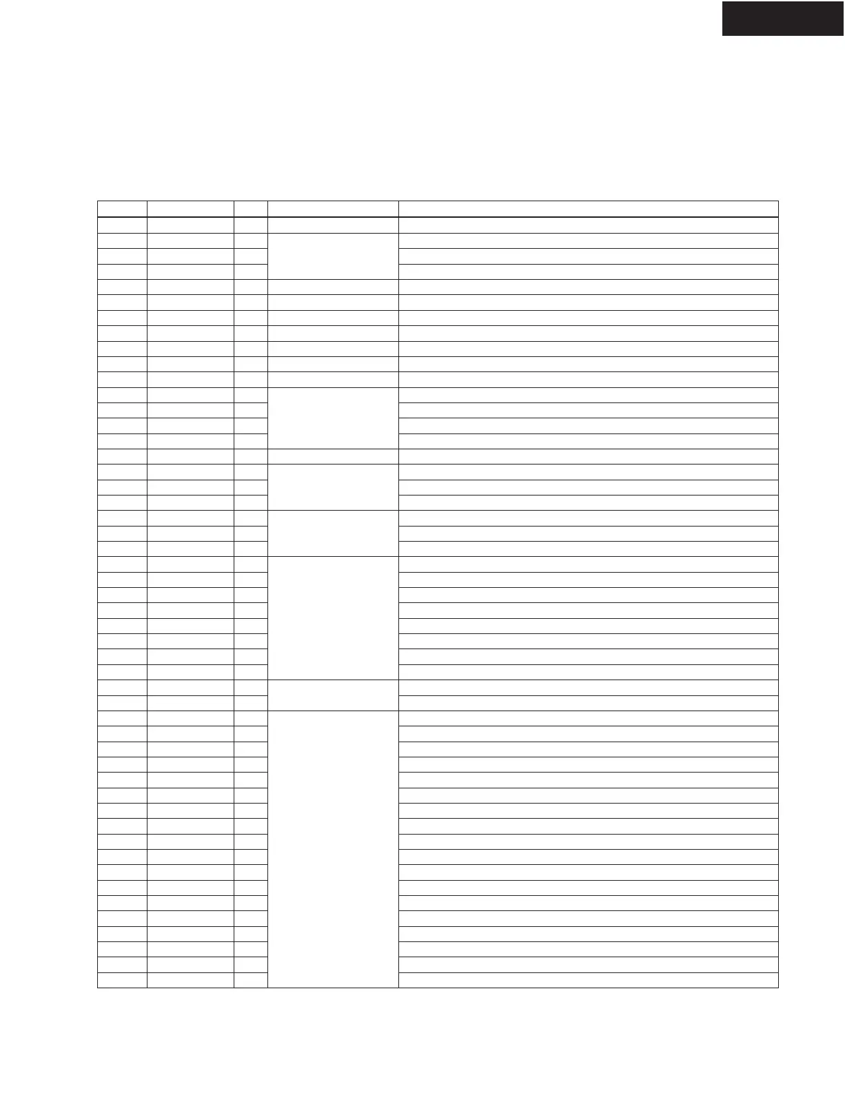
DX-C390
IC BLOCK DIAGRAM/ TERMINAL DESCRIPTION
Q501 : LC78683E MP3 DECODER FOR CD
Pin Functions
Pin No. Pin Name I/O Block Function
1 LRSY I CD IF CD left/right clock input
2 ADDATA O Audio data output
3 ADBCK O Audio bit clock output
4 ADLRCK O
Audio interface
Audio left/right clock output
5 C2FIN I CD IF CD C2 error flag input
6 TEST1 I Test Test input 1 (This pin must be connected to ground during normal operation.)
7 CKIN I CLOCK System clock input (16.9344 MHz)
8 VSS Power supply Ground
9 CKOUT O CLOCK External digital filter and D/A converter clock (384 fs) output
10 TEST2 I Test Test input 2 (This pin must be connected to ground during normal operation.)
11 DV
DD
1 Power supply Digital I/O system power supply
12 PW I CD subcode data serial input
13 SBSY I CD subcode block sync signal input
14 SFSY I CD subcode frame sync signal input
15 SBCK O
Subcode interface
CD subcode transfer serial clock output
16 AV
DD
Power supply Analog system (PLL) power supply
17 VPRFR VCO oscillator range setting
18 VCOC I VCO control voltage input
19 VPDO O
PLL
VCO charge pump output
20 AVSS Analog system ground
21 DV
DD
2 Internal logic system power supply
22 VSS
Power supply
GND
23 MDATA0 I/O DRAM data bus 0
24 MDATA1 I/O DRAM data bus 1
25 MDATA2 I/O DRAM data bus 2
26 MDATA3 I/O DRAM data bus 3
27 MDATA4 I/O DRAM data bus 4
28 MDATA5 I/O DRAM data bus 5
29 MDATA6 I/O DRAM data bus 6
30 MDATA7 I/O
Memory interface
DRAM data bus 7
31 DV
DD
3 Digital I/O system power supply
32 VSS
Power supply
GND
33 MDATA8 I/O DRAM data bus 8
34 MDATA9 I/O DRAM data bus 9
35 MDATA10 I/O DRAM data bus 10
36 MDATA11 I/O DRAM data bus 11
37 MDATA12 I/O DRAM data bus 12
38 MDATA13 I/O DRAM data bus 13
39 MDATA14 I/O DRAM data bus 14
40 MDATA15 I/O DRAM data bus 15
41 RASB O RAS output (active low)
42 WEB O WE output (active low)
43 CASLB O CAS output (lower byte, active low)
44 CASUB O CAS output (upper byte, active low)
45 OEB O OE output (active low)
46 MADRS12 O DRAM address output 12
47 MADRS11 O DRAM address output 11
48 MADRS10 O DRAM address output 10
49 MADRS9 O DRAM address output 9
50 MADRS8 O
Memory interface
DRAM address output 8
Continued on next page.
Analog system ground
 Loading...